The 286 Gives Up One Of Its Final Secrets

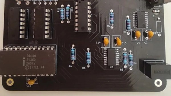
Though it is largely forgotten today, the Intel 80286 was for a while in the 1980s the processor of choice and designated successor to the 8086 in the world of PCs. It brought a new mode that could address up to 16 Mb of memory, and a welcome speed boost over machines using an 8086 or 8088. As with many microprocessors, it has a few undocumented features, and it’s a couple of these that [rep lodsb] takes a look at. Along the way we learn a bit about the 286, and about why Intel had some of these undocumented instructions in the first place.

If you used a 286 it was probably as an end-user sitting in front of a PC-AT or clone. During manufacture and testing though, the processor had need of some extra functions, both for testing the chip itself and for debugging designs using it. It’s in these fields that the undocumented instructions sit, and they relate to an in-circuit emulator, a 286 with a debug port on some of its unused pins, which would have sat on a plug-in daughterboard for systems under test. The 286 was famous for its fancy extended mode taking rather a long time to switch to, and these instructions relate to loading and saving states before and after the switch.

The 286s time as the new hotness was soon blasted away by the 386 with its support for virtual memory, so for most of us it remains as simply a faster way that we ran 8086 code for a few years. They appear from time to time here, even being connected to the internet.

286 image: Thomas Nguyen (PttNguyen.net), CC BY-SA 4.0.

Down The Intel Microcode Rabbit Hole

The aptly-named [chip-red-pill] team is offering you a chance to go down the Intel rabbit hole. If you learned how to build CPUs back in the 1970s, you would learn that your instruction decoder would, for example, note a register to register move and then light up one register to write to a common bus and another register to read from the common bus. These days, it isn’t that simple. In addition to compiling to an underlying instruction set, processors rarely encode instructions in hardware anymore. Instead, each instruction has microcode that causes the right things to happen at the right time. But Intel encrypts their microcode. Of course, what can be encrypted can also be decrypted.

Using vulnerabilities, you can activate an undocumented debugging mode called red unlock. This allows a microcode dump and the decryption keys are inside. The team did a paper for OffensiveCon22 on this technique and you can see a video about it, below.

Continue reading “Down The Intel Microcode Rabbit Hole”

How The IBM PC Went 8-Bit

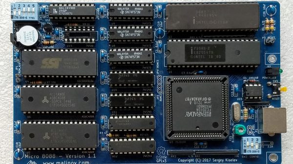
If you were around when the IBM PC rolled out, two things probably caught you by surprise. One is that the company that made the Selectric put that ridiculous keyboard on it. The other was that it had an 8-bit CPU onboard.  It was actually even stranger than that. The PC sported an 8088 which was a 16-bit 8086 stripped down to an 8 bit external bus. You have to wonder what caused that, and [Steven Leibson] has a great post that explains what went down all those years ago.

Before the IBM PC, nearly all personal computers were 8-bit and had 16-bit address buses. Although 64K may have seemed enough for anyone, many realized that was going to be a brick wall fairly soon. So the answer was larger address buses and addressing modes.

Intel knew this and was working on the flagship iAPX 432. This was going to represent a radical departure from the 8080-series CPUs designed from the start for high-level languages like Ada. However, the radical design took longer than expected. The project started in 1976 but wouldn’t see the light of day until 1981. It was clear they needed something sooner, so the 8086 — a 16-bit processor clearly derived from the 8080 was born. Continue reading “How The IBM PC Went 8-Bit”

AVX-512: When The Bits Really Count

For the majority of workloads, fiddling with assembly instructions isn’t worth it. The added complexity and code obfuscation generally outweigh the relatively modest gains. Mainly because compilers have become quite fantastic at generation code and because processors are just so much faster, it is hard to get a meaningful speedup by tweaking a small section of code. That changes when you introduce SIMD instructions and need to decode lots of bitsets fast. Intel’s fancy AVX-512 SIMD instructions can offer some meaningful performance gains with relatively low custom assembly.

Like many software engineers, [Daniel Lemire] had many bitsets (a range of ints/enums encoded into a binary number, each bit corresponding to a different integer or enum). Rather than checking if just a specific flag is present (a bitwise and), [Daniel] wanted to know all the flags in a given bitset. The easiest way would be to iterate through all of them like so:

while (word != 0) {
  result[i] = trailingzeroes(word);
  word = word & (word - 1);
  i++;
}

The naive version of this look is very likely to have a branch misprediction, and either you or the compiler would speed it up by unrolling the loop. However, the AVX-512 instruction set on the latest Intel processors has some handy instructions just for this kind of thing. The instruction is vpcompressd and Intel provides a handy and memorable C/C++ function called _mm512_mask_compressstoreu_epi32.

The function generates an array of integers and you can use the infamous popcnt instruction to get the number of ones. Some early benchmark testing shows the AVX-512 version uses 45% fewer cycles. You might be wondering, doesn’t the processor downclock when wide 512-bite registers are used? Yes. But even with the downclocking, the SIMD version is still 33% faster. The code is up on Github if you want to try it yourself.

SGX Deprecation Prevents PC Playback Of 4K Blu-ray Discs

This week Techspot reported that DRM-laden Ultra HD Blu-ray Discs won’t play anymore on computers using the latest Intel Core processors. You may have skimmed right past it, but the table on page 51 of the latest 12th Generation Intel Core Processor data sheet (184 page PDF) informs us that the Intel Software Guard Extensions (SGX) have been deprecated. These extensions are required for DRM processing on these discs, hence the problem. The SGX extensions were introduced with the sixth generation of Intel Core Skylake processors in 2015, the same year as Ultra HD Blu-ray, aka 4K Blu-ray. But there have been numerous vulnerabilities discovered in the intervening years. Not only Intel, but AMD has had similar issues as we wrote about in October.

This problem only applies to 4K Blu-ray discs with DRM. Presumably any 4K discs without DRM will still play, and of course you can still play the DRM discs on older Intel processors. Do you have a collection of DRM 4K Blu-ray discs, and if so, do you play them via your computer or a stand-alone player?

Peering Into The Murky Depths Of Alder Lake

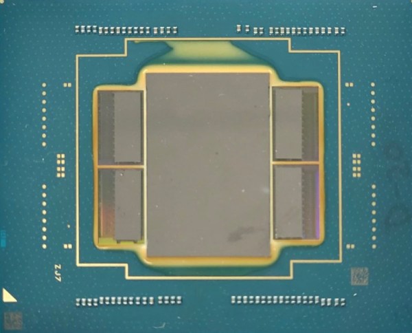
The winds of change are in the air for CPUs. Intel has long lorded over the computing world, and they remain a force to contend with, but many challengers gather at their gates. AMD, ARM, IBM, and other X86 designs sense a moment of weakness. In response, Intel released their Alder Lake platform with high-performance and high-efficiency cores, known as Golden Cove and Gracemont, respectively. [Clamchowder] and [cheese] have written up as many details as they were able to suss out about Gracemont.

ARM has done a multi-multi core design (big.LITTLE) for several years where they have a mix of high-power, high-performance cores and smaller, low-power cores. This allows the scheduler to make tradeoffs between power and performance. Typically the smaller cores in an ARM design are simpler in-order processors, having more in common with a microcontroller than with a full-scale desktop core. Many people have made an obvious comparison with the apparent similarities between ARM’s approach and Intel’s new offerings as Gracemont is based on Intel’s old Atom core, a low-power single issue, in-order processor. Continue reading “Peering Into The Murky Depths Of Alder Lake”

Intel RealSense D435 Depth Camera

RealSense No Longer Makes Sense For Intel

We love depth-sensing cameras and every neat hack they enabled, but this technological novelty has yet to break through to high volume commercial success. So it was sad but not surprising when CRN reported that Intel has decided to wind down their RealSense product line.

As of this writing, one of the better confirmations for this report can be found on the RealSense SDK GitHub repository README. The good news is that core depth-sensing RealSense products will continue business as usual for the foreseeable future, balanced by the bad news that some interesting offshoots (facial authentication, motion tracking) will be declared “End of Life” immediately and phased out over the next six months.

This information tells us while those living out on the bleeding edge will have to scramble, there is no immediate crisis for everyone else, whether they be researchers, hobbyists, or product planners. But this also means there will be no future RealSense cameras, kicking off many “What’s Next?” discussions in various communities. Like this thread on ROS (Robot Operating System) Discourse.

Three popular alternatives offer distinctly different tradeoffs. The “Been Around The Block” name is Occipital, with their more expensive Structure Pro sensor. The “Old Name, New Face” option is Microsoft Azure Kinect, the latest non-gaming-focused successor to the gaming peripheral that started it all. And let’s not forget OAK-D as the “New Kid On The Block” that started with a crowdfunding campaign and building an user community by doing things like holding contests. Each of these will appeal to a different niche, and we’ll keep our eye open in the future. Let’s see if any of them find the success that eluded the original Kinect, Google’s Tango, and now Intel’s RealSense.

[via Engadget]