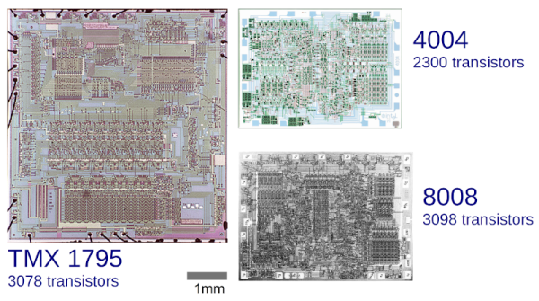
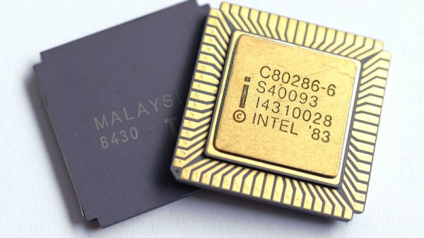
Intel’s Forgotten 1970s Dual Core Processor

Can you remember when you received your first computer or device containing a CPU with more than one main processing core on the die? We’re guessing for many of you it was probably some time around 2005, and it’s likely that processor would have been in the Intel Core Duo family of chips. With a dual-core ESP32 now costing relative pennies it may be difficult to grasp in 2020, but there was a time when a multi-core processor was a very big deal indeed.

What if we were to tell you that there was another Intel dual-core processor back in the 1970s, and that some of you may even have owned one without ever realizing it? It’s a tale related to us by [Chris Evans], about how a team of reverse engineering enthusiasts came together to unlock the secrets of the Intel 8271.

If you’ve never heard of the 8271 you can be forgiven, for far from being part of the chip giant’s processor line it was instead a high-performance floppy disk controller that appeared in relatively few machines. An unexpected use of it came in the Acorn BBC Micro which is where [Chris] first encountered it. There’s very little documentation of its internal features, so an impressive combination of decapping and research was needed by the team before they could understand its secrets.

As you will no doubt have guessed, what they found is no general purpose application processor but a mask-programmed dual-core microcontroller optimized for data throughput and containing substantial programmable logic arrays (PLAs). It’s a relatively large chip for its day, and with 22,000 transistors it dwarfs the relatively svelte 6502 that does the BBC Micro’s heavy lifting. Some very hard work at decoding the RMO and PLAs arrives at the conclusion that the main core has some similarity to their 8048 architecture, and the dual-core design is revealed as a solution to the problem of calculating cyclic redundancy checks on the fly at disk transfer speed. There is even another chip using the same silicon in the contemporary Intel range, the 8273 synchronous data link controller simply has a different ROM. All in all the article provides a fascinating insight into this very unusual corner of 1970s microcomputer technology.

As long-time readers will know, we have an interest in chip reverse engineering.

Odyssey Is A X86 Computer Packing An Arduino Along For The Trip

We love the simplicity of Arduino for focused tasks, we love how Raspberry Pi GPIO pins open a doorway to a wide world of peripherals, and we love the software ecosystem of Intel’s x86 instruction set. It’s great that some products manage to combine all of them together into a single compact package, and we welcome the recent addition of Seeed Studio’s Odyssey X86J4105.

[Ars Technica] recently looked one over and found it impressive from the perspective of a small networked computer, but they didn’t dig too deeply into the maker-friendly side of the product. We can look at the product documentation to see some interesting details. This board is larger than a Raspberry Pi, but its GPIO pins were laid out in exactly the same order as that on a Pi. Some HATs could plug right in, eliminating all the electrical integration leaving just the software issue of ARM vs x86. Tasks that are not suitable for CPU-controlled GPIO (such as generating reliable PWM) can be offloaded to an on-board Arduino-compatible microcontroller. It is built around the SAMD21 chip, similar to the Arduino MKR and Arduino Zero but the pinout does not appear to match any of the popular Arduino form factors.

The Odyssey is not the first x86 single board computer (SBC) to have GPIO pins and an onboard Arduino assistant. LattePanda for example has been executing that game plan (minus the Raspberry Pi pin layout) for the past few years. We’ve followed them since their Kickstarter origins and we’ve featured creative uses here and there. LattePanda’s current offerings are built around Intel CPUs ranging from Atom to Core m3. The Odyssey’s Celeron is roughly in the middle of that range, and the SAMD21 is more capable than the ATmega32U4 (Arduino Leonardo) on board a LattePanda. We always love seeing more options in a market for us to find the right tradeoff to match a given project, and we look forward to the epic journeys yet to come.

Reverse Engineering The Charge Pump Of An 8086 Microprocessor

You’d think that the 8086 microprocessor, a 40-year-old chip with a mere 29,000 transistors on board that kicked off the 16-bit PC revolution, would have no more tales left to tell. But as [Ken Shirriff] discovered, reverse engineering the chip from die photos reveals some hidden depths.

The focus of [Ken]’s exploration of the venerable chip is the charge pump, a circuit that he explains was used to provide a bias voltage across the substrate of the chip. Early chips generally took this -5 volt bias voltage from a pin, which meant designers had to provide a bipolar power supply. To reduce the engineering effort needed to incorporate the 8086 into designs, Intel opted for an on-board charge pump to generate the bias voltage. The circuit consists of a ring oscillator made from a trio of inverters, a pair of transistors, and some diodes to act as check valves. By alternately charging a capacitor and switching its polarity relative to the substrate, the needed -5 volt bias is created.

Given the circuit required, it was pretty easy for [Ken] to locate it on the die. The charge pump takes up a relatively huge amount of die space, which speaks to the engineering decisions Intel made when deciding to include it. [Ken] drills down to a very low level on the circuit, with fascinating details on how the MOSFETs were constructed, and why eight transistors were used instead of two diodes. As usual, his die photos are top quality, as are his explanations of what’s going on down inside the silicon.

If you’re somehow just stumbling upon [Ken]’s body of work, you’re in for a real treat. To get you started, you’ll want to check out how he found pi baked into the silicon of the 8087 coprocessor, or perhaps his die-level exploration of different Game Boy audio chips.

Intel Says Nanowire And NanoRibbon In Volume In Five Years

Intel’s CTO says the company will eventually abandon CMOS technology that has been a staple of IC fabrication for decades. The replacement? Nanowire and nanoribbon structures. In traditional IC fabrication, FETs form by doping a portion of the silicon die and then depositing a gate structure on top of an insulating layer parallel to the surface of the die. FinFET structures started appearing about a decade ago, in which the transistor channel rises above the die surface and the gate wraps around these raised “fins.” These transistors are faster and have a higher current capacity than comparable CMOS devices.

However, the pressure of producing more and more sophisticated ICs will drive the move away from even the FinFET. By creating the channel in multiple flat sheets or multiple wires the gate can surround the channel on all sides leading to even better performance. It also allows finer tuning of the transistor characteristics.

Continue reading “Intel Says Nanowire And NanoRibbon In Volume In Five Years”

Disable Intel’s Backdoor On Modern Hardware

While the Intel Management Engine (and, to a similar extent, the AMD Platform Security Processor) continues to plague modern computer processors with security risks, some small progress continues to be made for users who value security of the hardware and software they own. The latest venture in disabling the ME is an ASRock motherboard for 8th and 9th generation Intel chips. (There is also a link to a related Reddit post about this project).

First, a brief refresher: The ME is completely removable on some computers built before 2008, and can be partially disabled or deactivated on some computers built before around 2013. This doesn’t allow for many options for those of us who want modern hardware, but thanks to a small “exploit” of sorts, some modern chipsets are capable of turning the ME off. This is due to the US Government’s requirement that the ME be disabled for computers in sensitive applications, so Intel allows a certain undocumented bit, called the HAP bit, to be set which disables the ME. Researchers have been able to locate and manipulate this bit on this specific motherboard to disable the ME.

While this doesn’t completely remove the firmware, it does halt all execution of code in a way that is acceptable for a large governmental organization, so if you require both security and modern hardware this is one of the few ways to achieve that goal. There are other very limited options as well, but if you want to completely remove the ME even on old hardware the process itself is not as straightforward as you might imagine.

Header image: Fritzchens Fritz from Berlin / CC0

Magnetic Bubble Memory Farewell Tour

There’s something both satisfying and sad about seeing an aging performer who used to pack a full house now playing at a local bar or casino. That’s kind of how we felt looking at [Craig’s] modern-day bubble memory build. We totally get, however, the desire to finish off that project you thought would be cool four decades ago and [Craig] seems to be well on the way to doing just that.

If you don’t recall, bubble memory was going to totally wipe out the hard drive industry back in the late 1970s and early 1980s. A byproduct of research on twistor memory, the technology relied on tiny magnetic domains or bubbles circulating on a thin film. Bits circulated to the edge of the film where they were read using a magnetic pickup. Then a write head put them back at the other edge to continue their journey. It was very much like the old delay line memories, but with tiny magnetic domains instead of pressure waves through mercury.

We don’t know where [Craig] got his Intel 7110 but they are very pricey nowadays thanks to their rarity. In some cases, it’s cheaper to buy some equipment that used bubble memory and steal the devices from the board. You can tell that [Craig] was very careful working his way to testing the full board.

Because these were state-of-the-art in their day, the chips have extra loops and would map out the bad loops. Since the bubble memory is nonvolatile, that should be a one time setup at the factory. However, in case you lost the map, the same information appears on the chip’s label. [Craig’s] first test was to read the map and compare it to the chip’s printed label. They matched, so that’s a great sign the chip is in good working order and the circuit is able to read, at least.

We’ve talked about bubble memory before along with many other defunct forms of storage. There were a few military applications that took advantage of the non-mechanical nature of the device and that’s why the Navy’s NEETS program has a section about them.

New Part Day: Battery-Less NFC E-Paper Display

Waveshare, known for e-ink components aimed at hobbyists among other cool parts, has recently released a very interesting addition to their product line. This is an enclosed e-ink display which gets updated over a wireless NFC connection. By that description, nothing head-turning, but the kicker is that there is no battery inside the device at all, as it harvests the energy needed from the wireless communication itself.

Just like wireless induction charging in certain smartphones, the communication waves involved in NFC can generate a small current when passing through a coil, located on this device’s PCB. Since microcontrollers and e-ink displays consume a very small amount of current compared to other components such as a backlit LCD or OLED display, this harvested passive energy is enough to allow the display to update. And because e-paper requires no power at all to retain its image, once the connection is ended, no further battery backup is needed.

The innovation here doesn’t come from Waveshare however, as in 2013 Intel had already demoed a very similar device to promising results. There’s some more details about the project, but it never left the proof of concept stage despite being awarded two best paper awards. We wonder why it hadn’t been made into a commercial product for 5 years, but we’re glad it’s finally here for us to tinker with it.

E-paper is notorious for having very low refresh rates when compared to more conventional screens, much more so when driven in this method, but there are ways to speed them up a bit. Nevertheless, even when used as designed, they’re perfectly suited for being used in clocks which are easy on the eyes without a glaring backlight.

[Thanks Steveww for the tip!]