You know about the Hackaday Superconference, right? It’s the greatest hardware con ever, and it’s happening on November 5+6. Details incoming shortly.
The Hackaday Retro Edition exists. It’s the Hackaday blog, HTML-1-izized for weird and old computers? Why did I do this? Because Google is the quickest page to load on a Powerbook 180. There’s a new Retro Success, this time coming from @LeSpocky and his Nokia 3109c phone from 2008.
This is your official notice. The Open Hardware Summit is less than a month away. It’s going down in Portland, OR. Why Portland? The Vaporwavescene, of course. Hackaday, Tindie, and the rest of the crew will be out in Portland next month getting the latest news on the state of Open Hardware. We won’t be sitting in church pews this year, but then again there is no lady made out of soap.
Speaking of OHS, [Dave] just solved all their problems. The ‘problem’ with Open Hardware, if you can call it that, is that people use it as a bullet point on a sales deck. That neat gear logo can be marketing wank, without any of the sources, schematics, or anything else that makes a project Open Hardware. Last year, OSHWA announced they would be creating a certification process, with a trademarked logo, so they can sue people who don’t post schematics and mechanical designs (slightly inaccurate, but that’s the jist of the program). [Dave] is suggesting keeping the cool gear logo, but adding letters the teeth of the gear to designate what makes something Open Hardware. Add an S for schematic, add a B for a BOM, sort of like the creative commons logo/license. Is it a good idea? If OSHWA keeps using the gear logo for the ‘official’ Open Hardware logo/designation, there’s no recourse for when people misuse it. I’m of several minds.
[Colin Furze] is famous for his zany builds. His latest Youtube is anything but. It’s a shed. Of course, it’s the entry for his underground bunker, but this is a quality shed with a concrete pad, a few bits to keep it off the ground, and insulation. The roof is slate (because why not?), but if your design decisions are based on the phrase, ‘you only live once,’ copper may be a better choice.
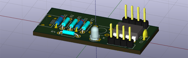
The ESP32 has been released. The ESP32 is the follow-on to the very popular ESP8266. The ’32 features WiFi and Bluetooth, dual core processors, and a few undisclosed things that will make it very interesting. You can buy ESP32 modules right now, but no one has them on their workbench quite yet. To get you started when they finally arrive, [Adam] created an ESP32 KiCad Library for the ESP32 chip, and the ESP32-WROOM and ESP3212 modules.