[KaZjjW] wanted to retrofit a pair of nicely styled vintage headphones to be able to play wirelessly over Bluetooth. In principle this is an easy task: simply stick a Bluetooth audio receiver on the line-in, add a battery, and you’re all set. However, [KaZjjW] wanted to keep the aesthetic changes to the headphones at an absolute minimum, retaining the existing casing and volume control, whilst cramming the electronics entirely inside and out of sight.
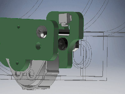
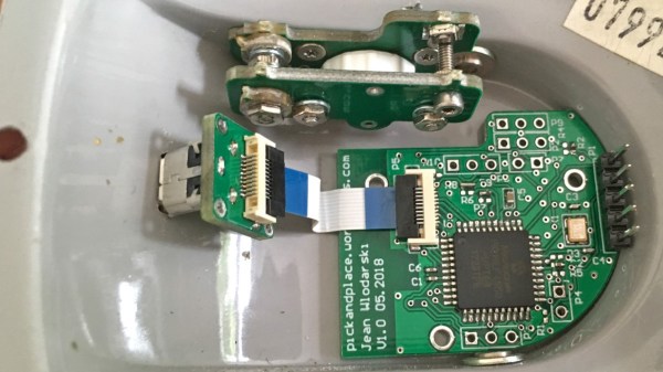
With the inherent space constraints inside the cups of the headphones, this proved to be quite a challenge. The existing volume potentiometer which hung half outside the case was remounted on an ingenious hinge made of two PCBs, with the pot floating next to a surface mounted switch. This allowed it to not only control the volume, but also act as an on/off switch for the Bluetooth. The only other existing cuts in the casing were a circular hole for the audio cable, and a slit for the cable strain relief. These worked perfectly for an LED status indicator and micro-USB battery charging.
The main chip used for receiving audio over Bluetooth was the BM62 by Microchip. It’s a great all-in-one solution for this kind of project as it has built-in battery charging, an on-board DAC and audio amp, as well as a serial control interface. In part 2 of the project log, the process of programming the BM62 was documented, and it was painful – it’s a shame that the software support lets it down. But a hacker will always find a way, and we’ve seen some pretty neat hacks for reprogramming existing chips in off-the-shelf Bluetooth headphones.
Two PCBs for the pot button hinge, one for the LED and micro-USB connector, as well as one for the Bluetooth receiver and a PIC. That’s four PCBs in a pretty small space, enabled by some commendable design effort both electronically and mechanically. It certainly paid off, as the finished product looks very slick.
Continue reading “Vintage Headphones Bluetooth Conversion Goes The Extra Mile”