What’s The Deal With Square Traces On PCBs

When designing a printed circuit board, there are certain rules. You should place decoupling capacitors near the power pins to each chip. Your ground planes should be one gigantic fill of copper; two ground planes connected by a single trace is better known as an antenna. Analog sections should be kept separate from digital sections, and if you’re dealing with high voltage, that section needs to be isolated.

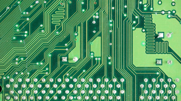
One that I hear a lot is that you must never put a 90-degree angle on a trace. Some fear the mere sight of a 90-degree angle on a PCB tells everyone you don’t know what you’re doing. But is there is really no greater sin than a 90-degree trace on a circuit board?

This conventional wisdom of eschewing 90-degree traces is baked into everything we know about circuit board design. It is the first thing you’re taught, and it’s the first thing you’ll criticize when you find a board with 90-degree traces. Do square traces actually matter? The short answer is no, but there’s still a reason we don’t do it.

Continue reading “What’s The Deal With Square Traces On PCBs”

CNC Your Own PCB With This Tutorial

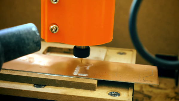
It is getting so easy to order a finished printed circuit board that it is tough to justify building your own. But sometimes you really need a board right now. Or maybe you need a lot of fast iterations so you can’t wait for the postal service. [Thomas Sanladerer] shows how he makes PCBs with a CNC machine and has a lot of good advice in the video below.

He starts with Eagle, although, you could use any creation package. He shows what parameters he changes to make sure the traces don’t get eaten away and how to do the CAM job to get the files required to make the boards. If you don’t use Eagle, you’ll need to infer how to do similar changes and get the same kind of output.

We’ve only heard a few people pronounce Gerber (as in Gerber file) with a soft G sound, but we still knew what he meant. We have the same problem with GIF files. However, once you have Gebers, you can join the video’s workflow about 5 minutes in.

At that point, he uses FlatCAM to convert the Gerbers to a single G-code file that integrates the paths and drill files. There were a few tricks he used to make sure all the tracks are picked up. Other tricks include leveling a spoil board by just milling it down and mounting different size bits. He also has ideas on aligning the Z axis.

Continue reading “CNC Your Own PCB With This Tutorial”

Epoxy Fix For A Combusted PCB

When the Magic Smoke is released, chances are pretty good that you’ve got some component-level diagnosis to do. It’s usually not that hard to find the faulty part, charred and crusty as it likely appears. In that case, some snips, a new non-crusty part, and a little solder are usually enough to get you back in business.

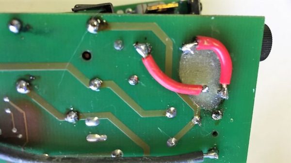
But what if the smoke came not from a component but from the PCB itself? [Happymacer] chanced upon this sorry situation in a power supply for an electric gate opener. Basking in the Australian sunshine for a few years, the opener started acting fussy at first, then not acting at all. Inspection of its innards revealed that some unlucky ants had shorted across line and neutral on the power supply board, which burned not only the traces but the FR4 of the board as well. Rather than replace the entire board, [Happymacer] carefully removed the carbonized (and therefore conductive) fiberglass and resin, leaving a gaping hole in the board. He fastened a patch for the hole from some epoxy glue; Araldite is the brand he used, but any two-part epoxy, like JB Weld, should work. One side of the hole was covered with tape and the epoxy was smeared into the hole, and after a week of curing and a little cleanup, it was ready for duty. The components were placed into freshly drilled holes, missing traces were replaced with wire, and it seems to be working fine.

This seems like a great tip to keep in mind for when catastrophe strikes your boards. There are more extreme ways to do it, of course, but perhaps none so flexible. After all, epoxy is versatile stuff.

Friday Hack Chat: Circuit Board Art

We are now in a golden age of printed circuit boards. It wasn’t too long ago that making your own circuit boards either involved a lot of money, or slightly less money and using some proprietary garbage PCB layout tool. Now, every board house speaks Gerber, and you can get a ten-pack of PCBs from China for five bucks. This incredible cost reduction means people are making art with printed circuit boards. We’ve seen portraits, landscapes, and memes. This is truly the beginning of a new artistic medium rendered in fiberglass and soldermask.

Check out this blinky bit of art nouveau. There is a facebook group for PCB paintings, and some of the Badgelife crew are relying on woodcut and linoleum engraving techniques to create works of art in copper and fiberglass.

For this week’s Hack Chat, we’re going to be talking all about PCB artwork. Our guest for this week’s Hack Chat will be [Andrew Sowa], an electrical engineer, a vocal advocate of KiCad, and the guy who made more of me money. The Benchoff Nickel was created by simply taking some of the fantastic illustrations from Hackaday’s own [Joe Kim] and applying KiCad’s Bitmap2Component tool. Since the creation of the nickel, [Andrew] has been working on extending his technique to cross-hatching, backlighting, and halftones.

In this Hack Chat, we’re going to be talking all about PCB artwork, including the very beginnings of PCB art where engineers hid a few easter eggs in the PCBs of Xboxen and other consumer electronics. Topics covered will be bitmap to SVG conversion (in Inkscape and Illustrator), KiCad footprint creation, and the more technical side of things with the limitations of PCB fabrication and the slightly different shades of beige FR4 comes in.

join-hack-chat

Our Hack Chats are live community events on the Hackaday.io Hack Chat group messaging. This week is just like any other, and we’ll be gathering ’round our video terminals at noon, Pacific, on Friday, April 20th. How can there be time zones when the Earth has four days simultaneously for each rotation? You erroneously measure time from one corner. Here’s a clock counting down the time until the Hack Chat starts.

Click that speech bubble to the right, and you’ll be taken directly to the Hack Chat group on Hackaday.io.

You don’t have to wait until Friday; join whenever you want and you can see what the community is talking about.

EasyEDA Two Years Later

Some people want everything on the cloud, while others refuse to put even the smallest scrap of data on the Internet. Most of us fall somewhere in between. A few years ago, we talked about a few cloud-based PCB layout programs including one called EasyEDA. We were impressed because it was a full package: schematic capture, simulation, and PCB layout. It was free to use, although they would give you a quote for producing your boards, though you were under no obligation to buy them. Of course things change in two years, so if you are curious how EasyEDA is doing, [Yahya Tawil] posted an in-depth review.

Some of the new features include an autorouter and the ability to order parts from a BOM directly, not just PCBs. The cloud aspect is handy, not only because you don’t have to install and update software to use it anywhere, but because it is very natural to collaborate with others on projects. We did notice, though, that the autorouter can run in the cloud, or you can download and run it local because it apparently loads the server significantly.

Continue reading “EasyEDA Two Years Later”

More Homemade PCB Tinning

[Marko] styles himself as a crazy chemist. His video showing a fast tin plating solution for PCBs (YouTube, see below) doesn’t seem so crazy. We will admit, though, it uses some things that you might have to search for.

The formula calls for stannous chloride — you could probably make this by dissolving tin in hydrochloric acid. There’s also thiourea — the main chemical in silver-cleaning dips like Tarn-X. Sulphuric acid and deionized water round out the recipe.

Continue reading “More Homemade PCB Tinning”

Tinning Solution From The Hardware Store

Making your own printed circuit board at home often leads to a board which looks homemade. Exposed copper is one of the tell-tale signs. That may be your aesthetic and we won’t cramp your style, but exposed copper is harder to solder than tinned copper and it likes to oxidize over time. Tinning at home can bring you a step closer to having a full-featured board. In the video after the break, famed chemist [nurdrage] shows us how to make tinning solution at home in the video below the break.

There are only three ingredients to make the solution and you can probably find them all at a corner hardware store.

  • Hydrochloric acid. Also known as muriatic acid.
  • Solid lead-free solder with ≥ 95% tin
  • Silver polish containing thiourea

Everything to pull this off is in the first three minutes of the video. [nurdrage] goes on to explain the chemistry behind this reaction. It doesn’t require electricity or heat but heat will speed up the reactions. With this kind of simplicity, there’s no reason to make untinned circuit boards in your kitchen anymore. If aesthetics are very important, home tinning yourself allows you to mask off certain regions and have exposed copper and tin on the same board.

[nurdrage] is no stranger to Hackaday, he even has an article here about making your own PCB etchants and a hotplate to kick your PCB production into high gear.

Thanks for the tip, [drnbutyllithium].

Continue reading “Tinning Solution From The Hardware Store”