3D Print A Stenciling Frame For Your PCB

For many a hacker, stenciling a board for the first time is a game-changing experience – the solder joints you get, sure do give your PCB the aura of a mass-manufactured device. Now, you might not get a perfect print – and neither did [Atul R]. Not to worry, because if you have a 3D printer handy, he’s showing you how to design a 3D-printed frame using Blender and TinkerCAD, making your solder paste print well even if you’re trying to rest a giant stencil on top of a tiny board.

[Atul]’s situation was non-characteristic – the project is a 2mm thick PCB designed to plug right into a USB port, so the usual trick of using some scrap PCBs wouldn’t work, and using a 3D-printed frame turned out to be key. To get it done, he exported a .wrl from KiCad, processed it in Blender, and then designed a frame with help of TinkerCAD. These techniques, no doubt, will translate into your CAD of choice – especially if you go with .step export instead of .wrl.

This kind of frame design will get you far, especially for boards where the more common techniques fail – say, if you need to assemble a double-sided board and one side is already populated. Don’t have a stencil? You could surely make a 3D printed stencil, too, both for KiCad boards and for random Gerber files. Oh, and don’t forget this 3D-printable stencil alignment jig, while you’re at it – looks like it ought to save you quite a bit of trouble.

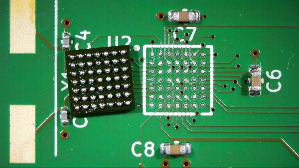
A freshly reballed BGA chip next to a clean PCB footprint

Working With BGAs: Soldering, Reballing, And Rework

In our previous article on Ball Grid Arrays (BGAs), we explored how to design circuit boards and how to route the signals coming out of a BGA package. But designing a board is one thing – soldering those chips onto the board is quite another. If you’ve got some experience with SMD soldering, you’ll find that any SOIC, TQFP or even QFN package can be soldered with a fine-tipped iron and a bit of practice. Not so for BGAs: we’ll need to bring out some specialized tools to solder them correctly. Today, we’ll explore how to get those chips on our board, and how to take them off again, without spending a fortune on equipment.

Tools of the Trade

For large-scale production, whether for BGA-based designs or any other kind of SMD work, reflow ovens are the tool of choice. While you can buy reflow ovens small enough to place in your workshop (or even build them yourself), they will always take up quite a bit of space. Reflow ovens are great for small-scale series production, but not so much for repairs or rework. Continue reading “Working With BGAs: Soldering, Reballing, And Rework”

Cameo Cutter Makes SMD Stencils

You never know what you might find in an arts and craft store. A relatively recent addition to crafting is automatic cutting machines like the Cricut and Cameo cutters. These are typically used to cut out shapes for scrapbooking, although they will cut or engrave almost anything thin. You can think of them as a printer with a cutting blade in place of the print head. [Mikeselectricstuff] decided to try a Cameo cutter to produce SMD stencils. The result, as you can see in the video below, is quite impressive.

If you’ve ever wanted to do SMD soldering with a reflow oven, stencils are invaluable for putting solder paste on the board where you want it quickly. The board [Mike] has contains a boat-load (over 2,000) of LEDs and dropping solder on each pad with a syringe would be very time consuming (although he did do some touch up with a syringe).

The board he’s using doesn’t have any extreme fine-pitched parts. However, he did some test patterns and decided he could get down to a finer pitch, especially with a little tweaking. However, the stencil he used didn’t need any changes. All he did was export the solder paste layer as a DXF and bring it straight into the Cameo software.

This isn’t the first time we’ve seen one of these cutters pressed into stencil service. You can also get some use out of your 3D printer.

Continue reading “Cameo Cutter Makes SMD Stencils”