Zork Comes To Custom FPGA CPU (Again)

[Robert Baruch] wanted to tackle a CPU project using an FPGA. One problem you always have is you can either mimic something that has tools and applications or  you can go your own way and just build everything from scratch (which is much harder).

[Robert] took the mimic approach–sort of. He built a CPU with the express idea of running Infocom’s Z-machine virtual machine, which allows it to play Zork. So at least when you are done, you don’t have to explain to your non-tech friends that it only blinks an LED. Check out the video, below, for more details.

Continue reading “Zork Comes To Custom FPGA CPU (Again)”

Retro ZX Spectrum Lives A Spartan Existence

FPGAs (like Xilinx’s Spartan series) are great building blocks. They often remind us of the 100-in-1 electronic kits we used to get as kids. Lots of components you can mix and match to make nearly anything. However, like a bare microcontroller, they usually don’t have much in the way of peripheral devices. So the secret sauce is what components you can surround the chip with.

If you are interested in retro computing, you ought to have a look at the ZX-Uno board. It hosts a Spartan 6 FPGA. They are for sale, but the design is open source and all the info is available if you prefer to roll your own or make modifications. You can see a video of the board in action, below (as explained in the video, the color issues are due to the capture card trying to deal with the non-standard sync rate).

Here are the key specifications:

  • FPGA Xilinx Spartan XC6SLX9-2TQG144C
  • Static Memory 512Kb, AS7C34096A-10TIN
  • 50MHz Oscillator
  • Video output (composite)
  • PS/2 keyboard
  • Stereo audio jack
  • EAR jack connector (for reading cassette tapes)
  • Connectors for JTAG and RGB
  • Slot for SD Cards
  • Expansion port with 3 male pin strips
  • Micro-USB power connector
  • PCB Size: 86×56 mm. (Compatible with Raspberry Pi cases)

Continue reading “Retro ZX Spectrum Lives A Spartan Existence”

Custom Zynq/CMOS Camera Unlocks Astrophotography

Around here we love technology for its own sake. But we have to admit, most people are interested in applications–what can the technology do? Those people often have the best projects. After all, there’s only so many blinking LED projects you can look at before you want something more.

[Landingfield] is interested in astrophotography. He was dismayed at the cost of commercial camera sensors suitable for work like this, so he decided he would create his own. Although he started thinking about it a few years ago, he started earnestly in early 2016.

The project uses a Nikon sensor and a Xilinx Zynq CPU/FPGA. The idea is the set up and control the CMOS sensor with the CPU side of the Zynq chip, then receive and process the data from the sensor using the FPGA side before dumping it into memory and letting the CPU take over again. The project stalled for a bit due to a bug in the vendor’s tools. The posts describe the problem which might be handy if you are doing something similar. There’s still work to go, but the device has taken images that should appear on the same blog soon.

Continue reading “Custom Zynq/CMOS Camera Unlocks Astrophotography”

Amstrad On An FPGA

If you are from the United States and of a certain age, it is very likely you owned some form of Commodore computer. Outside the US, that same demographic was likely to own an Amstrad. The Z80-based computers were well known for game playing. [Freemac] implemented a working Amstrad CPC6128 using a Xilinx FPGA on a NEXYS2 demo board.

The wiki posting is a bit long, but it covers how to duplicate the feat, and also gives technical details about the design. It also outlines the development process used ranging from starting with a simple Z80 emulation and moving on to more sophisticated attempts. You can see a video of the device below.

Continue reading “Amstrad On An FPGA”

DIYing Huge BGA Packages

One day [Andy] was cruising around eBay and spotted something interesting. Forty Virtex-E FPGAs for two quid each. These are the big boys of the FPGA world, with 512 user IO pins, almost 200,000 logic gates, packed into a 676-ball BGA package. These are not chips designed for the hobbyist. These chips are not designed for boards with less than six layers. These chips aren’t even designed for boards with 6/6mil tolerances from the usual suspects in China. By any account, a 676-ball package is not like a big keep out sign for hobbyists. You don’t turn down a £2 class in advanced PCB design, though, leading to one of the most impressive ‘I just bought some crap on eBay’ projects we’ve seen.

halfbuilt
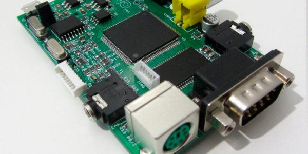
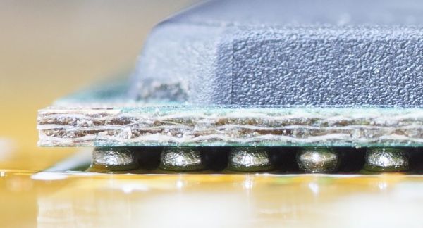
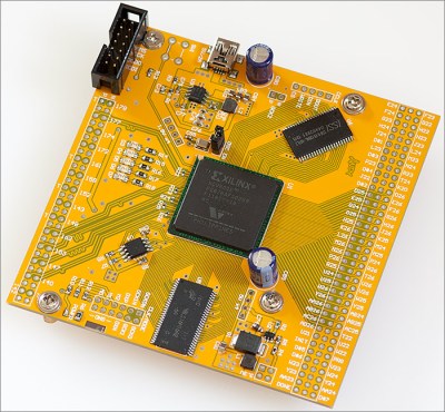
The project [Andy] had in mind for these chips was a generic dev board, which meant breaking out the IO pins and connecting some SRAM, SDRAM, and Flash memory. The first issue with this project is escape routing all the balls. Xilinx published a handy application note that recommends specific design parameters for the traces of copper under the chip. Unfortunately, this was a six-layer board, and the design rules in the application note were for 5/5mil traces. [Andy]’s board house can’t do six-layer boards, and their design rules are for 6/6mil traces. To solve this problem, [Andy] just didn’t route the inner balls, and hoped the 5mil traces would work out.

With 676 tiny little pads on a PCB, the clocks routed, power supply implemented, too many decoupling caps on the back, differential pairs, static RAM, a few LEDs placed just for fun, [Andy] had to solder this thing up. Since the FPGA was oddly one of the less expensive items on the BOM, he soldered that first, just to see if it would work. It did, which meant it was time to place the RAM, Flash, and dozens of decoupling caps. Everything went relatively smoothly – the only problem was the tiny 0402 decoupling caps on the back of the board. This was, by far, the hardest part of the board to solder. [Andy] only managed to get most of the decoupling caps on with a hot air gun. That was good enough to bring the board up, but he’ll have to figure some other way of soldering those caps for the other 30 or so boards.

Continue reading “DIYing Huge BGA Packages”

Rumors Of Xilinx Sale Abound

The companies that design and build the chips we all use – Atmel, Texas Instruments, Microchip, NXP, Freescale, Intel, Altera, Avago, Broadcom, and On Semi are all buying each other, merging, and slowly becoming two or three gigantic semiconductor companies. The question on everyone’s mind is, ‘which company will be next?’ The answer might be Xilinx, inventors of the FPGA and designers of some really cool parts.

The Wall Street Journal and Barron’s reported a few regulatory filings from Xilinx last week. This could signal an acquisition or merger of the company When this could happen is anyone’s guess, but rumors are flooding the Internet over who would buy Xilinx.

Until recently, Xilinx’s largest competitor in the FPGA market was Altera. That is, until Intel came by with a check for $16.7 Billion. The revenue, size, and market cap of both Xilinx and Altera aren’t too different, leading the question of who would have the money to buy Xilinx and isn’t Intel. Aren’t rumors fun?

Xilinx’s portfolio include high performance, mid-range and low-cost FPGAs as well as interesting hybrid devices. One such hybrid is Zynq, an FPGA and fast ARM Cortex A9 processor in the same package. All these chips will be made for years to come in one form or another. The only question is if Xilinx will make these chips, or will the company continue on under some new branding.

Zedboard Multiport Ethernet

The Zedboard uses Xilinx’s Zynq, which is a combination ARM CPU and FPGA. [Jeff Johnson] recently posted an excellent two-part tutorial covering using a Zedboard with multiple Ethernet ports. The lwIP (light-weight Internet Protocol) stack takes care of the software end.

Vivado is Xilinx’s software for configuring the Zynq (among other chips), and the tutorial shows you how to use it. The Ethernet PHY is an FPGA Mezzanine Card (FMC) with four ports that is commercially available. The project uses VHDL, but there is no VHDL coding involved, just the use of canned components.

The real issue when using an FPGA and a CPU is the interface between the processor and the FPGA circuitry. In this case, the ARM standard AXI bus does this task, and the Ethernet component properly interfaces to that bus. The IP application in the second part of the post is an echo server.

We’ve seen the Zynq used in flying machines and also in a music synthesizer. Although this project doesn’t use any Verilog or VHDL that you create, it is still a great example of configuring using Vivado and using common components in a design.