Proper Routing Makes For Many Happy Return Paths

Here’s a question for you: when your PCB has a ground plane layer, where do return signals flow? It seems like a trick question, but as [Kristof Mulier] explains, there’s more to return path routing (alternate link in case you run into a paywall) than just doing a copper pour and calling it a day.

Like so many other things in life, the answer to the above question is “it depends,” and as [Kristof] ably demonstrates in this concise article, the return path for a signal largely depends on its frequency. He begins by explaining current loop areas and how they factor into the tendency for a circuit to both emit and be susceptible to electromagnetic noise. The bigger the loop area, the worse things can get from a noise perspective. At low frequencies, return signals will tend to take the shortest possible path, which can result in large current loop areas if you’re not careful. At higher frequencies, though, signals will tend to follow the path of minimal energy instead, which generally ends up being similar to the signal trace, even if it has a huge ground plane to flow through.

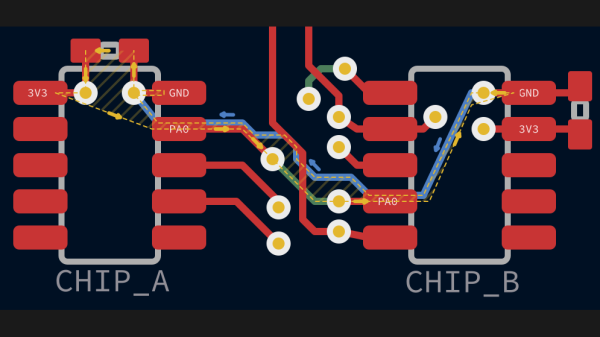
Since high-frequency signals naturally follow a path through the ground plane that minimizes the current loop, that means the problem takes care of itself, right? It would, except that we have a habit of putting all kinds of gaps in the way, from ground plane vias to isolation slots. [Kristof] argues that this can result in return paths that wiggle around these features, increasing the current loop area to the point where problems creep in. His solution? Route all your signal return paths. Even if you know that the return traces are going to get incorporated into a pour, the act of intentionally routing them will help minimize the current loop area. It’s brilliantly counterintuitive.

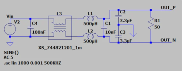
This is the first time we’ve seen the topic of high-frequency return paths tackled. This succinct demonstration shows exactly how return path obstructions can cause unexpected results.

Thanks to [Marius Heier] for the tip.

The Perils Of Return Path Gaps

The radio frequency world is full of mysteries, some of which seem to take a lifetime to master. And even then, it seems like there’s always something more to learn, and some new subtlety that can turn a good design on paper into a nightmare of unwanted interference and unexpected consequences in the real world.

As [Ken Wyatt] aptly demonstrates in the video below, where you put gaps in return paths on a PCB is one way to really screw things up. His demo system is simple: a pair of insulated wires running from the center pins on BNC jacks and running along the surface of a piece of copper-clad board to simulate a PCB trace. The end of each wire is connected to the board’s ground plane through a 50 ohm resistor, with one wire running over a narrow slot cut into the board. A harmonics-rich signal is fed into each trace while an H-field EMC probe connected to a spectrum analyzer is run along the length of the trace.

With the trace running over the solid ground plane, the harmonics are plentiful, as expected, but they fall off very quickly away from the trace. But over on the trace with the gapped return trace it’s a far different story. The harmonics are still there, but they’re about 5 dBmV higher in the vicinity of the gap. [Ken] also uses the probe to show just how far from the signal trace the return path extends to get around the gap. And even worse, the gap makes it so that harmonics are detectable on the unpowered trace. He also uses a current probe to show how common-mode current will radiate from a long conductor attached to the backplane, and that it’s about 20 dB higher with the gapped trace.

Hats off to [Ken] for this simple explanation and vivid reminder to watch return paths on clock traces and other high-frequency signals. Need an EMC probe to check your work? A bit of rigid coax and an SDR are all you needContinue reading “The Perils Of Return Path Gaps”

Homebrew TEM Cell Lets You EMC Test Your Own Devices

Submitting a new device for electromagnetic compatibility (EMC) testing seems a little like showing up for the final exam after skipping all the lectures. You might get lucky and pass, but it really would have been smarter to take a few of the quizzes to see how things were going during the semester. Similarly, it would be nice to know you’re not making any boneheaded mistakes early in the design process, which is what this DIY TEM cell is all about.

We really like [Petteri Aimonen]’s explanation of what a TEM cell, or transverse electromagnetic cell, is: he describes it as “an expanded coaxial cable that is wide enough to put your device inside of.” It basically a cage made of conductive material that encloses a space for the device under test, along with a stripline going down its center. The outer cage is attached to the outer braid of a coaxial cable, while the stripline is connected to the center conductor. Any electric or magnetic field generated by the device inside the cage goes down the coax into your test instrument, typically a spectrum analyzer.

[Petteri]’s homebrew TEM is made from a common enough material: copper-clad FR4. You could use double-sided material, or even sheet copper if you’re rich, but PCB stock is easy to work with and gets the job done. His design is detailed in a second post, which goes through the process of designing the size and shapes of all the parts as well as CNC milling the sheets of material. [Petteri] tried to make the joints by milling part-way through the substrate and bending the sheet into shape, but sadly, the copper didn’t want to cooperate with his PCB origami. Luckily, copper foil tape and a little solder heal all wounds. He also incorporated a line impedance stabilization network (LISN) into the build to provide a consistent 50-ohm characteristic impedance.

How does it work? Pretty well, it seems; when connected to a TinySA spectrum analyzer, [Petteri] was able to find high-frequency conductive noise coming from the flyback section of a switch-mode power supply. All it took was a ferrite bead and cap to fix it early in the prototyping phase of the project. Sounds like a win to us.

Aesthetic PCB Design Tips For Improved Functionality

Those of us hardware types that spend a lot of time designing PCBs will often look at other peoples’ designs with interest, and in some cases, considerable admiration. Some of their boards just look so good. But are aesthetics important? After all, for most products, the delicate electronic components on that PCB are tucked safely inside a protective enclosure. But, as [Phil’s Lab] explains, aesthetic PCB designs can lead to functional improvements, such that better-looking designs are also better performing, in terms of manufacturability (and therefore yield), electromagnetic compatibility (EMC), and several other factors that can be important.

First off, making a PCB easy to read and using sane placement of components and connections will speed up debugging by reducing errors. Keeping a consistent and not too-tight placement grid can give the pick and place machine an easier task, and reduce solder issues during reflow. But there are also more serious concerns, such as the enforcement of design partitionings — such as keeping analog circuits together and away from noisy power and digital areas — which can make the difference between functioning within specification, and failure.

The video goes into a few other interesting tips, one highlight is using a ground-tied PCB perimeter zone, with wavelength-of-interest via stitching. This will reduce EMC side emissions from the power plane, but also if you select an appropriate surface finish, and keep the solder mask open, you’ve got a free, full perimeter contact to ground your scope probe. Oh, and it looks good too.

Hackaday is no stranger to beautiful artistic PCBs, like the work of [Saar Drimer] and many others. But if one PCB doesn’t cut it for your needs, there’s always the ‘Oreo’ construction to consider.

Continue reading “Aesthetic PCB Design Tips For Improved Functionality”

EMC Tutorial Puts You In The Loop

A student once asked his lab instructor why his amplifier was oscillating. After looking at it and noting the wild construction, the instructor remarked, “A better question would be why shouldn’t it oscillate?” The truth of it is, our circuits generate noise and especially if they are oscillating anyway. Distortion and nonlinearities generate harmonics and other component imperfections also contribute.

[FesZ Electronics] has a great video series about noise in switching power supplies and the latest talks about the hot loop. If you want to improve the noise performance of your next design, these videos are well worth watching. You can see the hot loop video below.

We really liked the homebrew noise probes. In addition to real-world probing. The video also observes circuit operation under simulation. Even if you don’t care about noise performance, there’s a lot of good information about basic switching power supply design here.

You can see the difference in a PCB that has a small hot loop versus a very small hot loop. Something to think about next time you are laying out a power supply board.

If you want to dive deeper into noise simulation, we have a good read on that for you. Or ditch simulation, and make your own cheap probe with an SDR dongle.

Continue reading “EMC Tutorial Puts You In The Loop”

Hackaday Links Column Banner

Hackaday Links: September 12, 2021

The last thing an astronaut or cosmonaut on the International Space Stations wants to hear from one of their crewmates is, “Do you smell plastic burning?” But that’s apparently what happened this week aboard the increasingly problematic spacecraft, as the burning smell and visible smoke spread from the Russian Zvezda module to the American side of town. The reports say it occurred while charging the station’s batteries, and we all know how dicey that can get. But apparently, the situation resolved itself somehow, as normal operations continued soon after the event. Between reports of cracks, air leaks, problems with attitude control, and even accusations of sabotage, the ISS is really starting to show its age.

Speaking of burning and batteries, normally a story about burning Tesla batteries wouldn’t raise our eyebrows much. But this story out of California introduces a potential failure mode for Tesla batteries that we hadn’t considered before. It seems a semi-truck with a load of Tesla batteries lost its brakes on Interstate 80 in the Sierra Nevada mountains and ended up flipping across the highway. Video from the scene shows the cargo, which looks like replacement batteries or perhaps batteries salvaged from wrecked cars, scattered across the highway on their shipping pallets. A fire was reported, but it’s not clear whether it was one of the batteries which had gotten compromised in the crash, or if it was something other than the batteries. Still, we hadn’t considered the potential for disaster while shipping batteries like that.

Attention all GNURadio fans — GRCon21 is rapidly approaching. Unlike most of the conferences over the last year and half, GRCon21 will actually be both live and online. We always love the post-conference dump of talks, which cover such a wide range of topics and really dive deeply into so many cool areas. We’re especially looking forward to the SETI talks, and we’re pleased to see our friend Hash, who was on the Hack Chat a while back, scheduled to talk about his smart-meter hacking efforts. The conference starts on September 20 and is being held in Charlotte, North Carolina, and virtually of course. If you attend, make sure to drop tips to your favorite talks in the tips line so we can share them with everyone.

We got a tip this week on a video about how 1/4-wave tuning stubs work. It’s a simple demonstration using a length of coax, a signal generator, and an oscilloscope to show how an unterminated feedline can reflect RF back to the transmitter, and how that can be used to build super-simple notch filters and impedance transformers. We love demos that make the mysteries of RF a little simpler — W2AEW’s videos come to mind, like this one on standing waves.

Continue reading “Hackaday Links: September 12, 2021”

Make Some Noise Or Simulate It, At Least

Noise is a fact of life, especially in electronic circuits. But on our paper schematics and just as often our simulations, there is no noise. If you are blinking an LED on a breadboard, you probably don’t care. But if you are working on something meatier, handling electrical noise gracefully is important and simulation can help you. [Ignacio de Mendizábal] has a great piece on simulating EMC filters using LTSpice that can get you started.

There are many ways of classifying noise and [Ignacio] starts with common-mode versus differential noise, where common-mode is noise with current flowing in the same direction without regard to the circuit’s normal operation, and differential noise having currents that flow in the opposite direction of normal current flow.

Continue reading “Make Some Noise Or Simulate It, At Least”