Spud guns are a staple of summertime fun for the maker set, especially on the Eagleland side of the pond, combining as they do two of our favourite things: firearms and calories. Nine out of ten Canadians agree that there’s nothing quite like a high-speed poutine– but judging by accent [Current Concept] is an American and so his potato cannon needed a little something extra that even the second amendment doesn’t protect: fully automatic firing, with a belt feed.
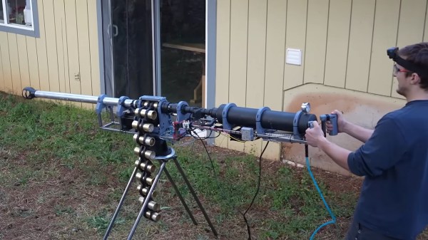
Like many spud guns, this one is powered by compressed air and uses PVC for both the barrel and air reservoir; unlike most spud guns, it has a steel frame holding it together, and a 3D-printed belt-feed mechanism to bring the spuds into position, with a beefy stepper motor pulling the potatoes. Of course just sticking an extra length of pipe between resivoire and barrel would just result in 80PSI potato-scented flatulence as the air escaped betwixt the gap, so a pair of piston-actuated, 3D printed fittings slides over the plastic casings in the belt that hold the spuds. It’s not a perfect seal, but video evidence suggests it’s tight enough to get the tubers flying. Finally, the whole thing was put on a bipod mount, because– uh. Look at it. It might be light enough for one man to carry, but this is clearly a crew-served weapon, even if there’s only one guy there.
Now, there are some caveats– the air reservoir is only good for one shot, so it needs to stay hooked to an air compressor to take advantage of the repeated firings. Since it has to recharge, it’s also only firing a spud every six seconds, so while the mechanism could do “full auto”, it’s actually semiautomatic in practice as nobody’s going to sit and hold the trigger that long. Finally, we must warn you that the YouTuber behind this is trying to be funny for much of the video. Some may find his delivery leaves them in stitches; others will be left cold. There is, of course, no accounting for taste.
Oddly enough, this isn’t the first automatic air gun to grace these pages. It’s also one of the weaker potato propellers, especially compared to this MAPP-gas powered monster. Hopefully [Current Concept] doesn’t see that and get any ideas for the promised revision of his belt-fed tuber tosser, or he may get a visit from the ATF– that’s the US Bureau of Alcohol, Tobacco, and Firearms, who are way less fun to deal with than the name might imply.
Continue reading “Belt Fed Potato Cannon Spits Spuds” →