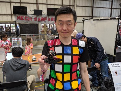
You can find all kinds of robots at Bay Area Maker Faire, but far and away the most interesting bot this year is the Self-Solving Rubik’s Cube built by [Takashi Kaburagi]. Gently mix up the colored sides of the cube, set it down for just a moment, and it will spring to life, sorting itself out again.
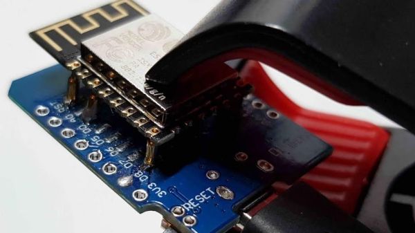
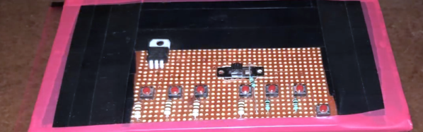
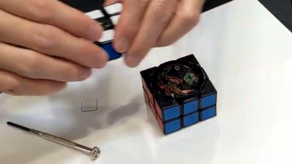
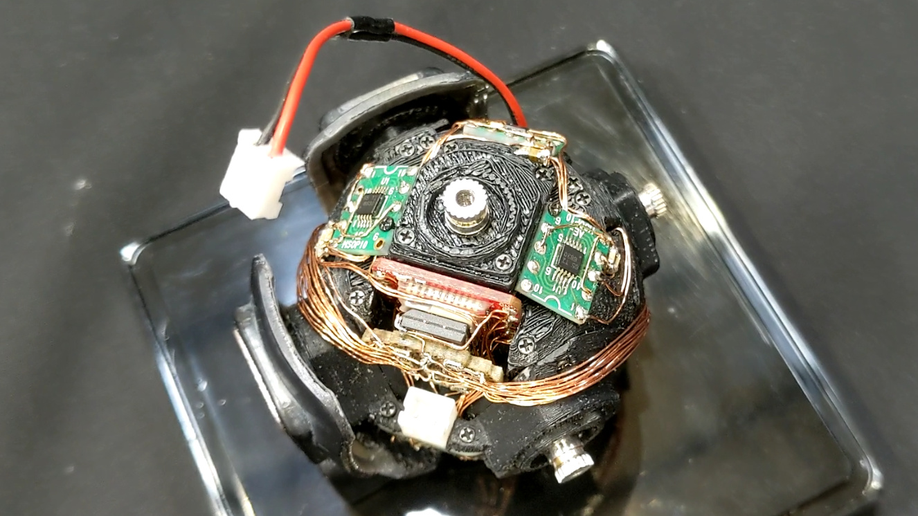
I arrived at [Takashi’s] booth at just the right moment: as the battery died. You can see the video I recorded of the battery swap process embedded below. The center tile on the white face of the cube is held on magnetically. Once removed, a single captive screw (nice touch!) is loosened to lift off the top side. From there a couple of lower corners are lifted out to expose the tiny lithium cell and the wire connector that links it to the robot.
Regular readers will remember seeing this robot when we featured it in September. We had trouble learning details about the project at the time, but since then Takashi has shared much more about what went into it. Going back to 2017, the build started with a much larger 3D-printed version of a cube. With proof of concept in hand, the design was modeled in CAD to ensure everything had a carefully planned place. The result is a hand-wired robotic core that feels like science fiction but is very, very real.
I love seeing all of the amazing robots on the grounds of the San Mateo County Event Center this weekend. There is a giant mech wandering the parking lot at the Faire. There’s a whole booth of heavy-metal quadruped bots the size of dogs. And if you’re not careful where you walk you’ll step on a scaled-down Mars rover. These are all incredible, out of this world builds and I love them. But the mental leap of moving traditional cube-solvers inside the cube itself, and the craftsmanship necessary to succeed, make this the most under-appreciated engineering at this year’s Maker Faire Bay Area. I feel lucky to have caught it during a teardown phase! Let’s take a look.
Continue reading “Teardown Video: What’s Inside The Self-Solving Rubik’s Cube Robot”