Hackaday 68k: A New Hackaday Project

It’s no secret Hackaday loves retrocomputers, classic hardware, and vintage tech. Now that we have a great way to present long-form projects, it only makes sense that we combine our loves with a new build. Over the next few months, I’ll be developing a homebrew computer based on the Motorola 68000 CPU, documenting everything along the way, and building a very capable piece of hardware that will end up hosting a few Hackaday webpages. I already have a solid start on the project and will be posting on our front page to discuss the major parts already in progress, and those yet to come.

There are a few reasons we’re taking on this project. With few exceptions, most of the homebrew projects we see are based around 8-bit micros – specifically the 6502 and Z80. 16 and 32-bit CPUs really aren’t that much more difficult to work with, and if we can spearhead a renaissance of the 68k, 65816, or even a 386 (!), we’re all for that. Also, it’s been suggested that we host the Hackaday Retro site on retro hardware, and what better way to do that by documenting a build on our new project hosting site?

That’s a very brief introduction to this project. Let’s take a closer look at what hardware we’ll be using, what software we’ll get running, and what you can do to help.

Continue reading “Hackaday 68k: A New Hackaday Project”

FT232RL: Real Or Fake?

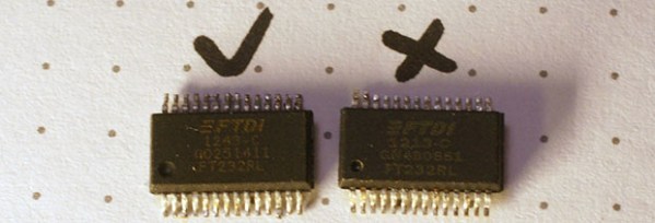
Above are two FTDI FT232RL chips, an extremely common chip used to add a USB serial port to projects, builds, and products. The one on the left is a genuine part, while the chip on the right was purchased from a shady supplier and won’t work with the current FTDI drivers. Can you tell the difference?

[Zeptobars], the folks behind those great die shots of various ICs took a look at both versions of the FT232 and the differences are staggering. Compared to the real chip, the fake chip has two types of SRAM etched in the silicon – evidence this chip was pieced together from different layouts.

The conclusion [Zeptobars] reached indicated the fake chip is really just a microcontroller made protocol compatable with the addition of a mask ROM. If you’re wondering if the FTDI chips in your part drawers are genuine, the real chips have laser engraved markings, while the clone markings are usually printed.

Expanded Memory For The Teensy++ 2.0

RAM

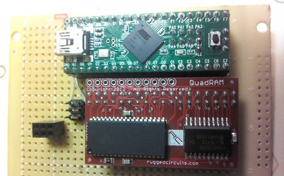
Sometimes with a microcontroller project you need to do some very RAM-hungry operations, like image and audio processing. The largish AVR chips are certainly fast enough to do these tasks, but the RAM on these chips is limited. [xxxajk] has come up with a library that allows the use of huge RAM expansions with the Teensy++ 2.0 microcontroller, making these RAM-dependant tasks easy on one of our favorite microcontroller board.

[xxajk]’s work is actually a port of XMEM2, an earlier project of his that added RAM expansion and multitasking to the Arduino Mega. Up to 255 banks of memory are available and with the supported hardware, the Teensy can address up to 512kB of RAM.

XMEM2 also features a preemptive multitasking with up to 16 tasks, the ability to pipe messages between tasks, and all the fun of malloc().

The build is fairly hardware independent, able to work with Rugged Circuits QuadRAM and MegaRAM expansions for the Arduino Mega as well as [Andy Brown]’s 512 SRAM expansion. With the right SRAM chip, etching a board at home for XMEM2 is also a possibility.

A Pick-And-Mix FPGA Retrocomputer

Logo

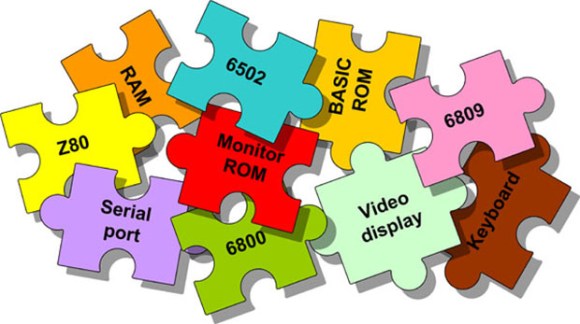
Cheap FPGA boards are readily available, as are VHDL implementations of classic CPUs like the 6502, 6809, and Z80. Up until now, we haven’t seen anyone take these two parts and combine them into a complete system that turns an FPGA board into a complete 8-bit retrocomputer. Thanks to [Grant]’s work, it’s now possible to do just that (server on fire, here’s a google cache) with a $30 FPGA board and a handful of parts.

In its full configuration, the Multicomp, as [Grant] calls his project, includes either a 6502, 6809, Z80, or (in the future) a 6800 CPU. Video options include either monochrome RCA, RGB VGA, or RGB via SCART. This, along an SD card interface, a PS2 keyboard, and the ability to connect an external 128kB RAM chip (64k available) means it’s a piece of cake to build a proper and complete portable retrocomputer.

What’s extremely interesting about [Grant]’s project is the fact the data and address lines are fully exposed on the FPGA board. This means it’s possible to add whatever circuit you’d like to whatever retrocomputer you can imagine; if you want a few NES gamepads, an IDE interface, or you’d like to design your own primitive video card, it’s just a matter of designing a circuit and writing some assembly.

If you’d like to build your own, search “EP2C5T144C8N” on the usual sites, grab a few resistors and connectors, and take a look at [Grant]’s documentation and upcoming examples.

Via 6502.org forums

An Easy Way To Power Flyback Transformers

FJISRREHR3EF3OP.LARGE

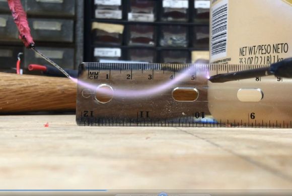
Let’s be honest. Playing with high voltage is awesome. Dangerous, but awesome — well, as long as you handle it properly. Flyback transformers are a great way to make a nice big electrical arc, but powering them isn’t that easy — or is it?

First off, for those that may not know, a flyback transformer is the type of transformer most commonly found in old TVs and CRT monitors. They typically can put out anywhere from 10kV to 50kV — the problem is, they aren’t that easy to power. Common methods include using a transistor style driver, or zero voltage switching (ZVS) — which is how [Skyy] cooked some s’mores at 50,000V.

As it turns out there’s another much easier and straight forward method. All you need is a fluorescent light ballast. Use the output on the ballast as the input on the primary winding of the flyback transformer — which can be found using a multimeter, just find the highest resistance between pins to identify it. Now because you’re working with such high voltages, you may want to insulate the flyback transformer by submerging it in mineral oil as to not short it out. That’s it.

Now it’s time to make some sparks.

Continue reading “An Easy Way To Power Flyback Transformers”

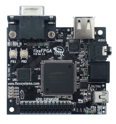
Introducing The FleaFPGA Experimenter’s Board

[Valentin] recently tipped us about an FPGA development board he just finished. It is called the FleaFPGA and is aimed to get people interested in the world of Field Programmable Gate Arrays. One of the other reasons that also got [Valentin] to design his own board was that he was frustrated with the existing solutions, them being either too pricey or fairly spare in terms of connectivity.

The main components that you can see in the platform shown above are: a lattice MachX02-7000HE FPGA (6864LUTs), 256Mbits of SDRAM, a USB2.0 host port, a 4096-color VGA connector, a 3.5mm stereo connector, an SD/MMC card slot, a PS/2 keyboard/mouse combo port, a few push buttons and LEDs. An expansion header is also present in order to connect the FleaFPGA to future shields that will be developed. Unfortunately only the board schematics have been released and [Valentin] is currently aiming for a price of $60 per board for <100 quantities. You’ll be able to see a video of the board in action after the break, in which the FPGA has been loaded with a 68000 software core running a variation of the Amiga Juggler Demo.

Continue reading “Introducing The FleaFPGA Experimenter’s Board”

Developed On Hackaday: The Current Project State

It has been quite a while since we updated our readers with the current state of the Mooltipass, the offline password keeper project developed by the Hackaday staff and community.

A few weeks ago we presented you the designs that our mechanical contributors had thought of. We organized a poll to get a feeling of what the favorite designs may be and around one thousand people expressed their opinions. The first three favorite designs with their corresponding votes were:

Continue reading “Developed On Hackaday: The Current Project State”