“You could’ve done that with a 555 timer.” But what if all you have on hand is an ESP8266? [TechColab] needed to control a solenoid valve with a short pulse via a solid-state relay (SSR) but found that the trusty 555 timer was tricky to set properly. Additionally, they wanted to add features, such as fixed pulse length, that were difficult to implement—even with multiple timers. Still wanting to keep things cheap and accessible, [TechColab] has created the WiFive55, a 555 replacement based on the ESP-01 ESP8266 board.
[TechColab] began by investigating existing ESP-01 solid-state relay boards but found that many of them momentarily enable the output on startup—a risk [TechColab] deemed unacceptable. This was resolved in the WiFive55 by adding an RC filter to the SSR output, eliminating the output glitches at the cost of slowing switching time to around 20 ms—an acceptable trade for many SSR applications.
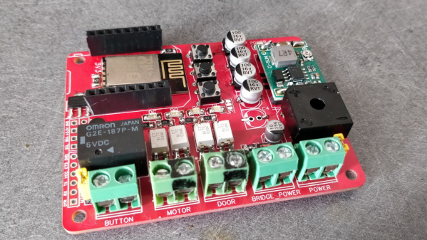
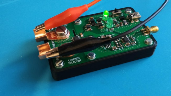
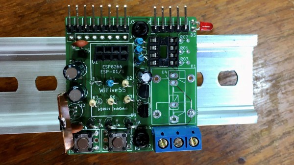
Since they were going to design a new PCB to support this improved ESP-01 SSR controller, [TechColab] decided to go all-out. To support loads of widely varying sizes, the PCB supports an optoisolator that switches up to 1 A, a MOSFET that switches up to 2 A, and an on-board relay or SSR that can switch up to 3 A. For heavy loads, it includes connections for an off-board SSR, which allow it to switch whatever current the SSR can handle (easily over 50 A). Because the ESP-01 is slightly more capable than the 555, the WiFive55 supports control via WiFi, GPIO, serial, and push-button. Keeping with the WiFive55’s original role as a 555 replacement, it even includes a header exposing a 555-like trigger and output interface!
We always like seeing inexpensive boards like the ESP-01 being used to their full potential, and we can’t wait to see what software [TechColab] cooks up for this! If you’re interested in getting started with the ESP-01, you might consider starting with this guide to blinking an LED over WiFi.