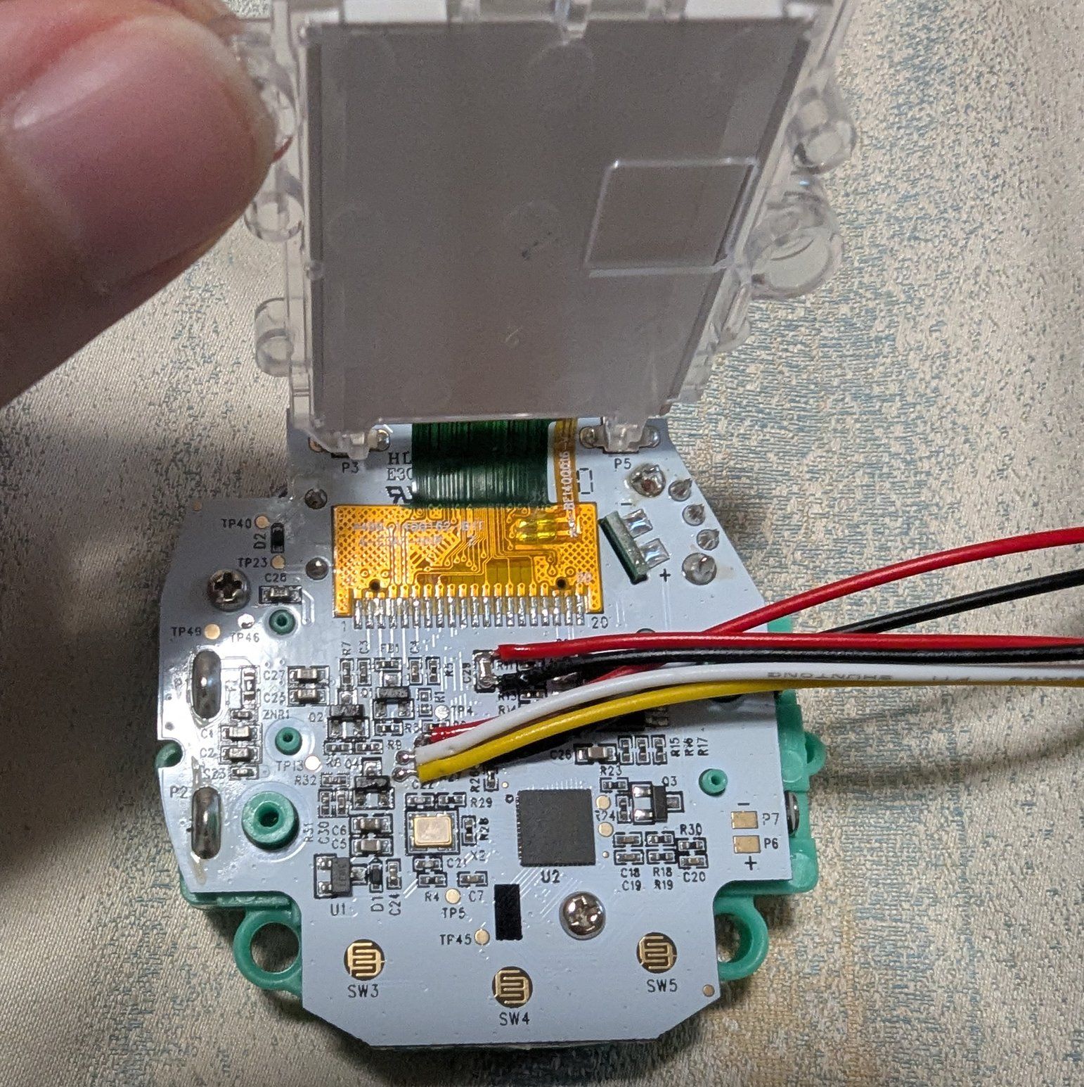
A Tricky Commodore PET Repair And A Lesson About Assumptions

The PET opened, showing the motherboard. (Credit: Ken Shirriff)

An unavoidable part of old home computer systems and kin like the Commodore PET is that due to the age of their components they will develop issues that go far beyond what was covered in the official repair manual, not to mention require unconventional repairs. A case in point is the 2001 series Commodore PET that [Ken Shirriff] recently repaired.

The initial diagnosis was quite straightforward: it did turn on, but only displayed random symbols on the CRT, so obviously the ICs weren’t entirely happy, but at least the power supply and the basic display routines seemed to be more or less functional. Surely this meant that only a few bad ICs and maybe a few capacitors had to be replaced, and everything would be fully functional again.

Initially two bad MOS MPS6540 ROM chips had to be replaced with 2716 EPROMs using an adapter, but this did not fix the original symptom. After a logic analyzer session three bad RAM ICs were identified, which mostly fixed the display issue, aside from a quaint 2×2 checkerboard pattern and completely bizarre behavior upon running BASIC programs.

Using the logic analyzer capture the 6502 MPU was identified as writing to the wrong addresses. Ironically, this turned out to be due to a wrong byte in one of the replacement 2716 EPROMs as the used programmer wasn’t quite capable of hitting the right programming voltage. Using a better programmer fixed this, but on the next boot another RAM IC turned out to have failed, upping the total of failed silicon to four RAM & two ROM ICs, as pictured above, and teaching the important lesson to test replacement ROMs before you stick them into a system.

The host stands in his electronics lab with the image of four remote controls overlaid.

Introducing Infrared Remote Control Protocols

Over on his YouTube channel [Electronic Wizard] has released a video that explains how infrared (IR) remote controllers work: IR Remote Controllers protocol: 101 to advanced.

This diagram indicates how the 38 kHz carrier wave is used to encode a binary signal.This video covers the NEC family of protocols, which are widely used in typical consumer IR remote control devices, and explains how the 38 kHz carrier wave is used to encode a binary signal.  [Electronic Wizard] uses his Rigol DS1102 oscilloscope and a breadboard jig to sniff the signal from an example IR controller.

There is also an honorable mention of the HS0038 integrated-circuit which can interpret the light waves and output a digital signal. Of course if you’re a tough guy you don’t need no stinkin’ integrated-circuit IR receiver implementation because you can build your own!

Before the video concludes there is a brief discussion about how to interpret the binary signal using a combination of long and short pulses. If this looks similar to Morse Code to you that’s because it is similar to Morse Code! But not entirely the same, as you will learn if you watch the video!

Hacking A Cheap Rechargeable Lamp With Non-Standard USB-C Connector

Recently [Dillan Stock] bought a $17 ‘mushroom’ lamp from his local Kmart that listed ‘USB-C rechargeable’ as one of its features. Unfortunately while this is technically true, there’s a pretty major asterisk. This Inaya-branded lamp comes with a USB-C cable with a rather prominent label attached to it that tells you that this lamp requires that specific cable. After trying with a regular USB-C cable, [Dillan] indeed confirmed that the lamp does not charge from a standard USB-C cable. So he did what any reasonable person would do: he bought a second unit and set about to hacking it.

The "USB C" cable that comes with the Inaya Portable Rechargeable Lamp. (Credit: The Stock Pot, YouTube)
The “USB C” cable that comes with the Inaya Portable Rechargeable Lamp. (Credit: The Stock Pot, YouTube)

[Dillan] also dug more into what’s so unusual about this cable and the connector inside the lamp. As it turns out, while GND & VCC are connected as normal, the two data lines (D+, D-) are also connected to VCC. Presumably on the lamp side this is the expected configuration, while using a regular USB-C cable causes issues. Vice versa, this cable’s configuration may actually be harmful to compliant USB-C devices, though [Dillan] did not try this.

With the second unit in hand, he started hacking in earnest. The changes include a regular USB-C port for charging, an ESP32 board with integrated battery charger for the 18650 Li-ion cell of the lamp, and an N-channel MOSFET to switch the power to the lamp’s LED. He’s made the full plans and schematics available on his website.

With all of the raw power from the ESP32 available, the two lamps got integrated into the Home Assistant network which enables features such as turning the lamps on when the alarm goes off in the morning. All of this took about $7 in parts and a few hours of work.

Although we commend [Dillan] on hacking his device instead of just returning it to the store, it’s worrying that apparently there’s now a flood of ‘USB C-powered’ devices out there that come with non-compliant cables. It brings back fond memories of hunting down proprietary charging cables, which was the issue that USB power was supposed to fix.

Continue reading “Hacking A Cheap Rechargeable Lamp With Non-Standard USB-C Connector”

A Toothbrush Hacked, In Three Parts

It’s official, we’re living in the future. Certainly that’s the only explanation for how [wrongbaud] was able to write a three-part series of posts on hacking a cheap electric toothbrush off of AliExpress.

As you might have guessed, this isn’t exactly a hack out of necessity. With a flair for explaining hardware hacking, [wrongbaud] has put this together as a practical “brush-up” (get it?) on the tools and concepts involved in reverse engineering. In this case, the Raspberry Pi is used as a sort of hardware hacking multi-tool, which should make it relatively easy to follow along.

Modified image data on the SPI flash chip.

The first post in the series goes over getting the Pi up and running, which includes setting up OpenOCD. From there, [wrongbaud] actually cracks the toothbrush open and starts identifying interesting components, which pretty quickly leads to the discovery of a debug serial port. The next step is harassing the SPI flash chip on the board to extract its contents. As the toothbrush has a high-res color display (of course it does), it turns out this chip holds the images which indicate the various modes of operation. He’s eventually able to determine how the images are stored, inject new graphics data, and write it back to the chip.

Being able to display the Wrencher logo on our toothbrush would already be a win in our book, but [wrongbaud] isn’t done yet. For the last series in the post, he shows how to extract the actual firmware from the microcontroller using OpenOCD. This includes how to analyze the image, modify it, and eventually flash the new version back to the hardware — using that debug port discovered earlier to confirm the patched code is running as expected.

If you like his work with a toothbrush, you’ll love seeing what [wrongbaud] can do with an SSD or even an Xbox controller.

Chip Glitching 101 With [Hash]

Ever want to get into reverse engineering but don’t know where to start? You’re in luck — [Hash] just dropped a case study in chip glitching that should get you off on the right foot.

The object of this reverse engineering effort in the video below is a Microchip SAM4C32C, removed from one of the many smart electrical meters [Hash] loves to tear into. This microcontroller was supposed to be locked to prevent anyone from sniffing around in the code, but after soldering the chip to a target board and plugging it into a Chip Whisperer, [Hash] was able to find some odd-looking traces on the oscilloscope. Of particular interest was an unusual pattern on the scope while resetting the chip, which led him to an AI-assisted search for potential vulnerabilities. This allowed him to narrow down the target time for a power glitch, and in only a few seconds, the chip was forced to bypass its security bit and drop into its boot loader. With the keys to the kingdom, [Hash] was able to read the firmware and find all sorts of interesting tidbits.

Obviously, chip glitching isn’t always as easy as this, and even when a manufacturer leaves a vector like this in the chip, exploiting it does take some experience and finesse. But, if you’re going to get started glitching, it makes sense to start with the low-hanging fruit, and having [Hash] along for the ride doesn’t hurt either.

Continue reading “Chip Glitching 101 With [Hash]”

Why Are Micro Center Flash Drives So Slow?

Every year, USB flash drives get cheaper and hold more data. Unfortunately, they don’t always get faster. The reality is, many USB 3.0 flash drives aren’t noticeably faster than their USB 2.0 cousins, as [Chase Fournier] found with the ultra-cheap specimens purchased over at his local Micro Center store.

Although these all have USB 3.0 interfaces, they transfer at less than 30 MB/s, but why exactly? After popping open a few of these drives the answer appears to be that they use the old-style Phison controller (PS2251-09-V) and NAND flash packages that you’d expect to find in a USB 2.0 drive.

Across the 32, 64, and 256 GB variants the same Phison controller is used, but the PCB has provisions for both twin TSOP packages or one BGA package. The latter package turned out to be identical to those found in the iPhone 8. Also interesting was that the two 256 GB drives [Chase] bought had different Phison chips, as in one being BGA and the other QFP. Meanwhile some flash drives use eMMC chips, which are significantly faster, as demonstrated in the video.

It would seem that you really do get what you pay for, with $3 “USB 3.0” flash drives providing the advertised storage, but you really need to budget in the extra time that you’ll be waiting for transfers.

Continue reading “Why Are Micro Center Flash Drives So Slow?”

The Pentium Processor’s Innovative (and Complicated) Method Of Multiplying By Three, Fast

[Ken Shirriff] has been sharing a really low-level look at Intel’s Pentium (1993) processor. The Pentium’s architecture was highly innovative in many ways, and one of [Ken]’s most recent discoveries is that it contains a complex circuit — containing around 9,000 transistors — whose sole purpose is to multiply specifically by three. Why does such an apparently simple operation require such a complex circuit? And why this particular operation, and not something else?

Let’s back up a little to put this all into context. One of the feathers in the Pentium’s cap was its Floating Point Unit (FPU) which was capable of much faster floating point operations than any of its predecessors. [Ken] dove into reverse-engineering the FPU earlier this year and a close-up look at the Pentium’s silicon die shows that the FPU occupies a significant chunk of it. Of the FPU, nearly half is dedicated to performing multiplications and a comparatively small but quite significant section of that is specifically for multiplying a number by three. [Ken] calls it the x3 circuit.

The “x3 circuit”, a nontrivial portion of the Pentium processor, is dedicated to multiplying a number by exactly three and contains more transistors than an entire Z80 microprocessor.

Why does the multiplier section of the FPU in the Pentium processor have such specialized (and complex) functionality for such an apparently simple operation? It comes down to how the Pentium multiplies numbers.

Multiplying two 64-bit numbers is done in base-8 (octal), which ultimately requires fewer operations than doing so in base-2 (binary). Instead of handling each bit separately (as in binary multiplication), three bits of the multiplier get handled at a time, requiring fewer shifts and additions overall. But the downside is that multiplying by three must be handled as a special case.

[Ken] gives an excellent explanation of exactly how all that works (which is also an explanation of the radix-8 Booth’s algorithm) but it boils down to this: there are numerous shortcuts for multiplying numbers (multiplying by two is the same as shifting left by 1 bit, for example) but multiplying by three is the only one that doesn’t have a tidy shortcut. In addition, because the result of multiplying by three is involved in numerous other shortcuts (x5 is really x8 minus x3 for example) it must also be done very quickly to avoid dragging down those other operations. Straightforward binary multiplication is too slow. Hence the reason for giving it so much dedicated attention.

[Ken] goes into considerable detail on how exactly this is done, and it involves carry lookaheads as a key element to saving time. He also points out that this specific piece of functionality used more transistors than an entire Z80 microprocessor. And if that is not a wild enough idea for you, then how about the fact that the Z80 has a new OS available?