
[Nagy Krisztián] had an Intel 286 CPU, only… There was no motherboard to install it in. Perhaps not wanting the processor to be lonely, [Nagy] built a simulated system to bring the chip back to life.
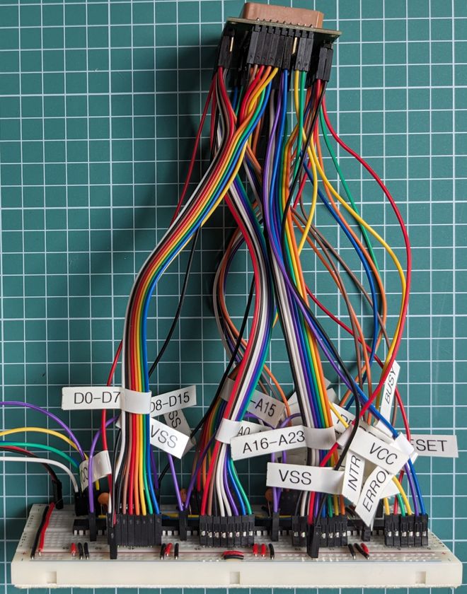
The concept is simple enough. [Nagy] merely intended to wire the 286 up to a Raspberry Pi Pico that could emulate other parts of a computer that it would normally expect to talk to. This isn’t so hard with an ancient CPU like the 286, which has just 68 pins compared to the 1000+ pins on modern CPUs. All it took was a PLCC-68 socket, an adapter PCB, a breadboard, and some MCP23s17 logic expanders to give the diminutive microcontroller enough I/O. With a bit of work, [Nagy] was able to get the Pi Pico running the 286, allowing it to execute a simple program that retrieves numbers from “memory” and writes them back in turn.
Notably, this setup won’t run the 286 at its full clock speed of 12 MHz, and it’s a long way off from doing anything complex like talking to peripherals or booting an OS. Still, it’s neat to see the old metal live again, even if it’s just rattling through a few simple machine instructions that don’t mean a whole lot. [Nagy] equates this project to The Matrix; you might also think of it as a brain in a jar. The 286 is not in a real computer; it’s just hooked up to a microcontroller stimulating its various pins in a way that is indistinguishable from its own perspective. Continue reading “Making A 286 Think It’s Alive Again”


