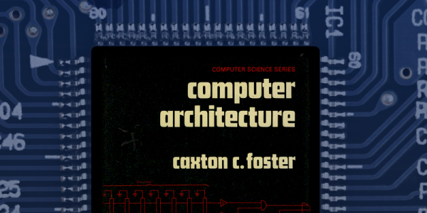
I’ve worked with a lot of students who want to program computers. In particular, a lot of them want to program games. However, when they find out that after a few weeks of work they won’t be able to create the next version of Skyrim or Halo, they often get disillusioned and move on to other things. When I was a kid, if you could get a text-based Hi-Lo game running, you were a wizard, but clearly the bar is a lot higher than it used to be. Think of the “Karate Kid”–he had to do “wax on, wax off” before he could get to the cool stuff. Same goes for a lot of technical projects, programming or otherwise.
I talk to a lot of people who are interested in CPU design, and I think there’s quite a bit of the same problem here, as well. Today’s commercial CPUs are huge beasts, with sophisticated memory subsystems, instruction interpreters, and superscalar execution. That’s the Skyrim of CPU design. Maybe you should start with something simpler. Sure, you probably want to start learning Verilog or VHDL with even simpler projects. But the gulf between an FPGA PWM generator and a full-blown CPU is pretty daunting.
Continue reading “Crawl, Walk, Run: Planning Your First CPU Design”

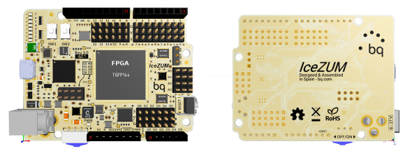
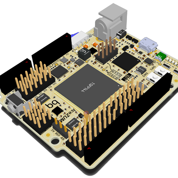
 enthusiasts around the world. To get it to the masses, they started an ambitious 2 million US dollar Indiegogo campaign, which has unfortunately come to a