Dummies Guide To Reverse Engineering

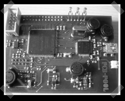
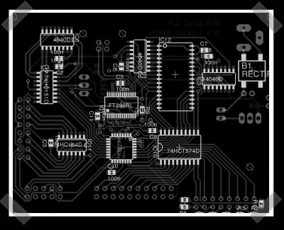
[Juan Carlos Jiménez] has reverse engineered a router — specifically, a Huawei HG533. While that in itself may not sound substantial, what he has done is write a series of blog posts which can act as a great tutorial for anyone wanting to get started with sniffing hardware. Over the five part series, he walks through the details of identifying the hardware serial ports which open up the doors to the firmware and looking at what’s going on under the hood.

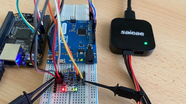
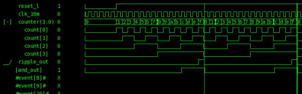
The first part deals with finding the one or several debug ports on the hardware and identifying the three important pins – Rx, Tx and GND. That’s when he shows novices his first trick – shining a flashlight from under the PCB to find the pins that have trace connections (most likely Rx and Tx), those that don’t have any connections (most likely CTS and DTR) and those that have connections to the copper pour planes (most likely VCC and GND). The Tx signal will be pulled up and transmitting data when the device is powered up, while the Rx signal will be floating, making it easy to identify them. Finding the Baud rate, though, will require either a logic analyser, or you’ll have to play a bit of a guessing game.

Once you have access to the serial port and know its baud rate, it’s time to hook it up to your computer and use any one of the several ways of looking at what’s coming out of there — minicom, PuTTY or TeraTerm, for example. With access to the devices CLI, and some luck with finding credentials to log in if required, things start getting interesting.

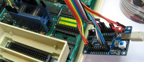
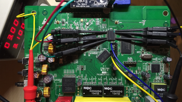
Over the next part, he discusses how to follow the data paths, in this case, looking at the SPI signals between the main processor and the flash memory, and explaining how to use the logic analyser effectively and decode the information it captures. Moving further, he shows how you can hook up a USB to SPI bridge, connect it to the flash memory, take a memory dump of the firmware and read the extracted data. He wraps it up by digging in to the firmware and trying to glean some useful information.

It’s a great series and the detailed analysis he does of this particular piece of hardware, along with providing a lot of general tips, makes it a perfect starting point for those who need some help when getting started on debugging hardware.

Thanks, [gnif] for posting this tip.

Continue reading “Dummies Guide To Reverse Engineering”

An Open Source 96 MSPS Logic Analyzer For $22

If you are in the market for an inexpensive USB logic analyser you have a several choices, but few of them deliver much in the way of performance. There are kits from China for a few dollars using microcontrollers at their heart, but they fail to deliver significant sample rates. If you require more, you will have to pay for it.

It is therefore rather interesting to see [kevinhub88]’s SUMP2 project, an open source logic analyser with a claimed 96 MSPS sample rate using an off-the-shelf Lattice iCEstick FPGA evaluation board that only costs about $20. It talks to a host computer via USB using the established SUMP protocol, so its software front-end comes from the sump.org logic analyser project. Edit: Since this post was published [Kevin] has contacted us to inform us that the project’s capabilities have now moved beyond SUMP’s capabilities and in fact it now uses his own software.

This project has the promise to add a very useful piece of test equipment to the armoury of the engineer on a budget, and to aid the cost-conscious reader he’s provided extensive documentation and installation instructions, as well as the code for the FPGA. Thanks to one of the more awesome hacks of 2015, there is an entirely open toolchain for this Lattice part, and our own [Al Williams] has written up a multi-part getting-started guide if you want to get your feet wet. You probably want one of these anyway, and now it’s a logic analyzer to boot.

We’ve covered quite a few inexpensive home-produced digital instruments here over the years, including this logic analyser with a slightly higher price tag, this inexpensive VNA, and this oscilloscope board. Maybe one day the bench of our dreams will all come on one open-source PCB for $100, who knows!

USB 2.0 FPGA Based 24 Channel Logic Analyzer


[lekernel] sent in his USB logic analyzer. I might just have to build this one for my work bench. It’s based on an Altera Cyclone 2 FPGA and he’s provided full schematics, source and a quick and dirty Linux driver to get things going. The board is nearly all surface mount, but he points out that the entire thing was soldered with a standard iron and de-soldering wick. If you’re looking for a good starter FPGA project, this looks like a good one.

I started writing for Hack-A-Day a little over a year ago. I’ve barely taken a break, but for the next week I’m going to be taking some serious time off on a Caribbean island. Thanks for a great year guys! While I’m gone, [fbz] has kindly consented to take over the reins. I’m looking forward to another year when I get back, but right now I’ve got to finish packing my dive gear.