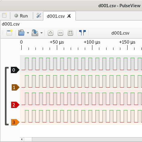
Saleae logic analyzers seem to have it all: good sampling rates, convenient protocol decoding, and plenty of channels – but not a good way to set rising or falling-edge triggering. [James] found this rather inconvenient when debugging embedded devices, and shared a workaround that replicates these simple triggering modes.
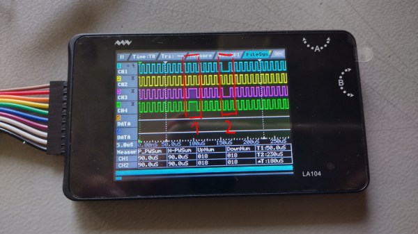
Crucially, the logic analyzer’s software has a repeated triggering mode that fires when the protocol decoder detects a preset value. [James] used a clever trick to turn this into a rising-edge trigger: he set up a simple parallel analyzer, and set the signal in question as both the sampled channel and the clock signal. Since he wanted to detect the rising edge, he set the clock mode accordingly. Next, he loaded the simple parallel decoder’s trigger configuration and set it to detect a value of one, the value of a high signal. When he ran the simple parallel trigger, every rising edge of the input signal would trigger the clock to check for a high value on the line, in turn triggering the analyzer.
It’s also possible to set up a falling-edge trigger by selecting the falling-edge clock mode and setting the trigger mode to detect a value of zero. Setting up more complex triggers involving multiple channels is as simple as calculating the hexadecimal value of the desired state and setting the parallel decoder to trigger on that value. For example, if you want to trigger when one input is low and another is high, you can set the decoder to trigger on a value or one or two, depending on which order the inputs come in.
If all this makes you interested in Saleae logic analyzers, we’ve seen them used for everything from floppy disk preservation to signal generation. We’ve even reviewed their earliest model back in 2009.
Continue reading “Simple Triggering For Saleae Logic Analyzers”