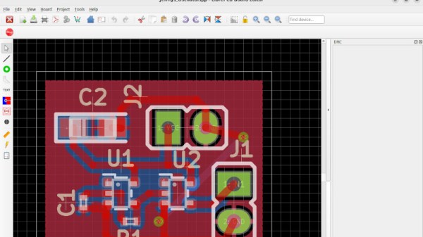
It’s like Star Wars versus Star Trek at a SciFi convention, or asking creamy or chunky at the National Peanut Butter Appreciation Festival. (OK, we made that one up.) When Jenny reviewed the 1.0 version of LibrePCB, it opened the floodgates. Only on Hackaday!
Of course it makes sense that in a community of hardware hackers, folks who are not unfamiliar with the fine art and engineering of designing their own PCBs, have their favorite tools. Let’s face it, all PCB design software is idiosyncratic, and takes some learning. But the more fluent you are with your tool of choice, the more effort you have invested in mastering it, leading to something like the sunk-cost phenomenon: because you’ve put so much into it, you can’t think of leaving it.
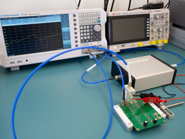
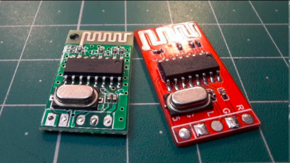
The beauty of open-source software tools is that there’s almost nothing, aside from your own psychology, stopping you from picking up another PCB program, kicking the proverbial tires with a simple design, and seeing how it works for you. That’s what Jenny did here, and what she’s encouraged me to do. Whether it’s beginner-friendly Fritzing (also recently in version 1.0), upstarts LibrePCB or Horizon EDA, heavyweight champion KiCAD, or the loose-knit conglomeration of tools in coralEDA, you have enough choices that something is going to fit your PCB hand like a glove.
I certainly wouldn’t risk a swap up to a new tool on something super complicated, or something with a tight deadline, but why not start up a fun project to test it out? Maybe follow Tom Nardi’s lead and make a Simple Add-on, for a badge or just as a blinky to put on your desk? Don’t be afraid to try something new!
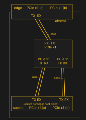 PCIe needs TX pairs connected to RX on another end, like UART – and this is non-negotiable. Connectors will use host-side naming, and vice-versa. As the diagram demonstrates, we connect the socket’s TX to chip’s RX and vice-versa; if we ever get confused, the laptop schematic is there to help us make things clear. To sum up, we only need to flip the names on the link coming to the PCIe switch, since the PCIe switch acts as a device on the card; the two links from the switch go to the E-key socket, and for that socket’s purposes, the PCIe switch acts as a host.