Repairing A Thermal Imaging Camera

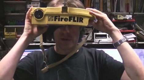
[Mike] got his hands on this thermal imaging camera which is designed for use by Firefighters. As he’s demonstrating in the image above, it clips to a helmet and has a display what will let rescuers see through heavy smoke. But this one isn’t working right so he cracked it open and repaired the damaged board.

The hour-long video (embedded after the break) is quite interesting. He starts with a disassembly of the unit, before diving head-first into trouble shooting. There is a PCB inside that fills the entire U-shaped enclosure. The thermal sensor’s habit of cutting out seems to be a symptom of this design. There is one weak point where the board is very narrow. Flexing or vibrating that section will reset the sensor, and [Mike] ends up replacing a couple of components before the thing is fixed. These include a resistor and a ferrite bead both of which are suspected of having cracks due to that board flexing. The rest of the video is spent with an EEVblog-style look that the components and the construction.

Continue reading “Repairing A Thermal Imaging Camera”

[Ladyada’s] Thoughts On Quick-turn And Small-run PCB Houses

So you’ve mastered your PCB layout software, and it’s time to make the board. But if you don’t want to etch your own you’ve got to decided where to have it fabricated. There’s a slew of services out there, most of which you cannot afford, but the short list of those you can is still pretty long. We think this set of PCB fabrication house reviews will help you make your choice.

[Ladyada] — aka [Limor Fried] — knows what she’s talking about. She owns Adafruit Industries and has done the lion’s share of designing the many kits and items they sell. If you’re going to charge money for something it better work right, and that involves lots of prototypes. But even if you don’t need a quick turn-around or numerous testing boards the post is helpful as she also covers some of the batch producers we’re already familiar with. These include DorkBot PDX and BatchPCB to name a couple.

[via Reddit]

Mantis9 PCB Mill

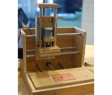
This is the Mantis9 PCB mill. It’s the first time we’ve featured the project, but it’s already well known by some as it keeps popping up in the comments for other CNC mill projects. Yes, it’s made out of wood — which some frown upon — but we’re happy with the build instructions and the especially the price tag (parts as low as $85).

We did feature an earlier revision of the hardware back in 2010. Subsequent versions changed the frame to use an open-front design, but it’s the build techniques that saw the biggest evolution. The problem was getting the holes for the parallel rods to align accurately. In the end it’s a simple operation that solves the problem; clamp both boards together and drill the holes at the same time. A drill press is used for all of the fabrication, ensuring that the holes are perpendicular to the surface of the boards. From there the rods are given some bronze bushings and pressed into place. Only then are the platforms secured to the bushings using epoxy. This is to ensure that the bushings don’t bind from poor alignment. We think it should end up having less play in it than other builds that use drawer slides.

Check out a PCB milling run in the clip after the break.

Continue reading “Mantis9 PCB Mill”

PCB Manufacturing Tutorial

There comes a time in every maker’s career where solderless breadboards won’t do, perfboard becomes annoying, and deadbug is impossible. The solution is to manufacture a PCB, but there’s a learning curve. After learning a few tricks from [Scott]’s awesome DIY PCB guide, it’s easy to make your own printed circuit boards.

There are a few basic steps to making a PCB. First is designing the board in Eagle or KiCad. The next step, putting the design into copper, has a lot of techniques to choose from. Photo transfer, direct printing, and CNC milling have huge benefits, but by far the most common means hobbyists produce boards is with toner transfer using a laminator.

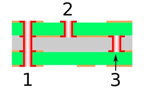
Unless you’re doing SMD-only circuits, a drill is required. Most people can get away with a Dremel or other rotary tool, but Hackaday has a favorite drill press that is perfect for drilling holes in FR-4. In part two of [Scott]’s tutorial, he goes over solder masks, silk screens before jumping into vias. These small bits of copper conducting electricity through a circuit board are extremely hard for the garage-bound builder to achieve on their own, but there are a few solutions – copper rivets (anyone have a US source for these?) and copper foil can be used, but sometimes the most effective solution is just hitting the board with a lot of solder and heat.

Thanks [Upgrayd] for the title pic.

3D Printed Circuit Boards Using Conductive Ink

The thought of using a 3D printer to fabricate PCBs is tantalizing and the good news is that it’s a reality. This project shows that it’s possible to use a special printer head to apply traces to an extruded substrate.

This is similar to the point-to-point 3D printer circuits with one big upgrade. Now the traces can be printed directly onto the ABS using conductive ink. The process starts with the design files, which are used to model a substrate that has a trench for each trace. A Makerbot then prints out this model. Once complete, the ABS extruder head is swapped for a special ink head. Each trace is then filled with the conductive fluid, which is kept in place by the trench walls until it can dry. We think this improves on the trace printing techniques we’ve seen before because it doesn’t require your printer heat to use molten metals.

The circuit above uses printed traces for the high and low side of an LED circuit. It’s a bit rough at the edges, but it shows a lot of promise. Don’t miss the demo video embedded after the jump.

Continue reading “3D Printed Circuit Boards Using Conductive Ink”

Going From Idea To Schematic To Printed PCB

Building a circuit on a bread board makes life much easier, but eventually you’re going to want a PCB for one of your circuits. Luckily, [Will] from Revolt Lab put up a trio of posts that will take you idea and turn it into a schematic and PCB.

First up is an awesome tutorial on the circuit design program Fritzing. While you won’t find Fritzing on the computer of anyone making a living doing circuit design work – those people usually go for Eagle or KiCad – Fritzing is very easy to use but still has a ton of features. Using Fritzing isn’t very hard, either. [Will]’s tutorial goes over copying your breadboarded circuit into Fritzing, creating a schematic from the bread board layout, and finally converting that to PCB artwork.

Once you have board artwork for your circuit, you’re probably going to want a real-life PCB. [Will]’s board etching tutorial goes over the toner transfer method of PCB creation. Basically, print your circuit onto glossy photo paper with a laser printer, put it face down on a copper board, then take a clothes iron to it. If you’re lucky, the laser printer toner will have transferred to the copper making a nice etch resist. To get rid of all that superfluous copper, [Will] used ferric chloride but a Hydrochloric Acid/Hydrogen Peroxide mix will work just as well.

Before you etch your boards, you might want to thing about building an etch tank that keeps all your slightly dangerous chemicals in one container. [Will]’s etch tank uses a large water container and a few pieces of LEGO to suspend the board in the etch solution. It etches boards a lot faster than laying them face down in a tray, allowing you to go from idea to finished piece a lot quicker.

Are Your PCBs Being Tested As Claimed?

Florin ordered some PCBs from Iteadstudio, a pcb prototyping service. As part of their service, they claim that all PCBs are tested before they are delivered. However, many have been bringing this claim into question. [Florin] found a complete lack of any markings indicating actual probes had been used on his boards. Though they claim that 100% of the boards are e-tested, they replied to his inquiry somewhat cryptically.

All of the pcb’s have a stripe on the edge,it does not mean they have all been electrically tested ,it is the same as outline .

People on the Dangerous Prototypes Forum have been finding similar results. The company has commented, on this page, that that they will be responding to this soon (back in February)