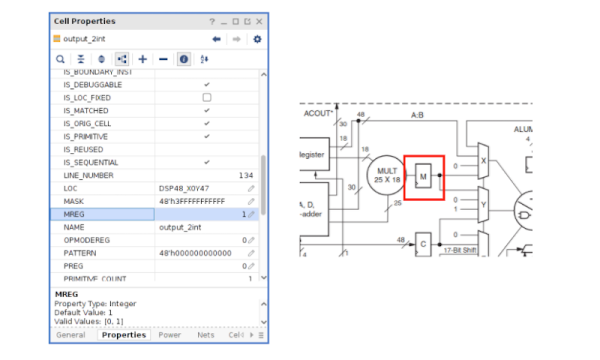
Digital filters are always an interesting topic, and they are especially attractive with FPGAs. [Pabolo] has been working with them in a series of blog posts. The latest covers an 8th order FIR filter in Verilog. He covers some math, which you can find in many places, but he also shows how an implementation maps to DSP slices in a device. Then to reduce the number of slices, he illustrates folding which trades delay time for slice usage.
Folding takes a multi-stage parallel multiplication and breaks it into fewer multiplications done over a longer period of time. This reuses slices to reduce the number required for high-order filters.
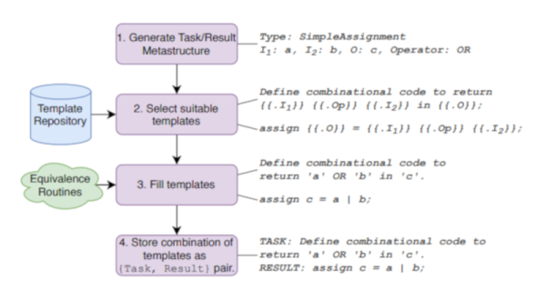
We were always envious of Star Trek, for its computers. No programming needed. Just tell the computer what you want and it does it. Of course, HAL-9000 had the same interface and that didn’t work out so well. Some researchers at NYU have taken a natural language machine learning system — GPT-2 — and taught it to generate Verilog code for use in FPGA systems. Ironically, they called it DAVE (Deriving Automatically Verilog from English). Sounds great, but we have to wonder if it is more than a parlor trick. You can try it yourself if you like.
For example, DAVE can take input like “Given inputs a and b, take the nor of these and return the result in c.” Fine. A more complex example from the paper isn’t quite so easy to puzzle out:
Write a 6-bit register ‘ar’ with input
defined as ‘gv’ modulo ‘lj’, enable ‘q’, synchronous
reset ‘r’ defined as ‘yxo’ greater than or equal to ‘m’,
and clock ‘p’. A vault door has three active-low secret
switch pressed sensors ‘et’, ‘lz’, ‘l’. Write combinatorial
logic for a active-high lock ‘s’ which opens when all of
the switches are pressed. Write a 6-bit register ‘w’ with
input ‘se’ and ‘md’, enable ‘mmx’, synchronous reset
‘nc’ defined as ‘tfs’ greater than ‘w’, and clock ‘xx’.
For most people, adding WiFi to a project means grabbing something like an ESP8266 or an ESP32. But if you are developing your own design on an FPGA, that means adding another package. If you are targeting Linux, the OpenWifi project has a good start at providing WiFi in Verilog. There are examples for many development boards and advice for porting to your own target on GitHub. You can also see one of the developers, [Xianjun Jiao], demonstrate the whole thing in the video below.
The demo uses a Xilinx Zynq, so the Linux backend runs on the Arm processor that is on the same chip as the FPGA doing the software-defined radio. We’ll warn you that this project is not for the faint of heart. If you want to understand the code, you’ll have to dig into a lot of WiFi trivia.
There’s a lot of argument over which was the first modern computer to be built. There’s room for debate, but EDSAC — the work of Dr. Maurice Wilkes — certainly was among the first. While we’ve seen simulators before, [hrvach’s] FPGA-based simulator for the MiSTer platform has a lot going for it. Check out the video, below.
So much of what we take for granted today was first developed on the EDSAC. For example, the “Wheeler jump” (named after graduate student David Wheeler) was the origin of the idea of a subroutine.
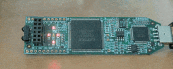
After trying out hardware hacking using an FPGA to interface with target hardware, [Grazfather] was inspired to try using the iCEBreaker (one of the many hobbyist FPGAs to have recently flooded the market) to build a UART-controllable glitcher for the Olimex LPC-P1343.
When the target board boots up, the bootROM reads the flash and determines whether the UART goes to a shell and if the shell can be used to read out the flash. This is meant for developing firmware and debugging it in the bootloader, only flashing a version when the firmware is production-ready. The vulnerability is that only a specific value read from address 0x2FC and the state of a few pins can lock the bootloader in the expected way, and any other value at the address causes the bootROM to consider the device unlocked. Essentially, the mechanism is the opposite of how a lock ought to work.
The goal is to get the CPU to misread the flash at the precise moment it is meant to be reading the specific value, then jumping to the bootloader in the unlocked state. The FPGA can be used as a tool between the host machine and target board, communicating via UART. The FGPA can support configuring the delay between resetting the target board and pulsing a ‘glitch voltage’, as well as resetting the target board and activating the glitch. The primary reasons for using the FPGA over a different microcontroller are that the FPGA allows for precise timing (83.3ns precision) and removes worries about jitters (a Raspberry Pi might have side effects from OS scheduling and other processes and microcontrollers might have interrupts messing up the timing).
To simulate the various modules, [Grazfather] used Icarus Verilog as well as GTKWave to observe the waveforms generated. A separate logic analyzer observes the effects on real hardware.
With enough time, it is possible to brute force any combination of delay and width until you get a dump of the flash you’re not meant to read. You can check out how the width of the pulse gets wider until the max, when the delay is incremented and the width values are tried again.
We always marvel at how open-source tools can often outstrip their commercial counterparts. Yosys, the open-source tool for Verilog synthesis, is a good example. Although the Xilinx ISE design suite is something close to abandonware, a lot of people still use it because it supports older FPGAs the newer tools don’t. Its Verilog parser is somewhat slow to catch up to new standards, and according to a recent GitHub update, Yosys can now provide files for ISE that target Spartan 6, Virtex 7, and Series 7 FPGAs. In addition, there is some support for Spartan 3, Virtex 2, 4, and 5, although those are not ready yet.
According to the post, you’ll want to use the synth_xilinx command along with the -ise option and a -family option that matches your target (that is, xc6s for Spartan 6). On the output side, you’ll write an EDIF file using the write_edif command.
When life hands you a ridiculously expensive and massively powerful FPGA dev board, your first reaction may not be to build a 16-core Z80 laptop with it. If it’s not, perhaps you should examine your priorities, because that’s what [Chris Fenton] did, with the result being the wonderfully impractical “ZedRipper.”
Our first impression is that we’ve got to start hanging around a better class of lab, because [Chris] came by this $6000 FPGA board as the result of a lab cleanout; the best we ever scored was a few old Cat-5 cables and some power strips. The Stratix FPGA formed the heart of the design, surrounded by a few breakout boards for the 10.1″ VGA display and the keyboard, which was salvaged from an old PS/2. The 16 Z80 cores running in the FPGA are connected by a ring-topology network, which [Chris] dubs the “Z-Ring”. One of the Z80 cores, the server core, runs CP/M 2.2 and a file server called CP/NET, while the other fifteen machines are clients that run CP/NOS. A simple window manager shows 80 x 25 character terminal sessions for the server and any three of the clients at once, and the whole thing, including a LiPo battery pack, fits into a laser-cut plywood case. It’s retro, it’s modern, it’s overkill, and we absolutely love it.