Quantum Atomic Interferometer For Precision Motion Sensing

The current state of the art of embedded motion sensing is based around micro-electromechanical systems (MEMS) devices. These miracles of microfabrication use tiny silicon structures, configured to detect acceleration and rotational velocity in three dimensions. Accumulate these accelerations and rotations, and you’ve got a device that can find its orientation and track movement without any external waypoints. This is the basis of the technique of dead reckoning.

Why do we care about dead reckoning anyway? Surely GPS and related positioning systems are good enough? Above ground GPS is usually good enough, but underwater and underground this simply won’t work. Even heading indoors has a dramatic effect on the GPS signal strength, so yes, we need another way for some applications.

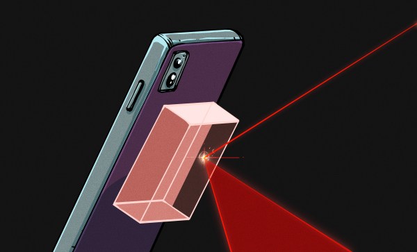
Right now, the current state of the art in portable sensors are MEMS devices, and you can get them for the cost of a hamburger. But if you want the ultimate in accuracy, you’ll want a quantum atomic interferometer. What that is, and how it will be possible to make one small enough to be useful, is half of the story. But first, let’s talk MEMS.

Continue reading “Quantum Atomic Interferometer For Precision Motion Sensing”

Laser doping silicon wafer

Laser Doping His Way To Homemade Silicon Chips

It’s a pity that more electronics enthusiasts haven’t taken the hobby to its ultimate level: making your own semiconductors. There are plenty of good reasons for that: chief among them is the huge expense involved in obtaining the necessary equipment. But for the sufficiently clever, there are ways around that.

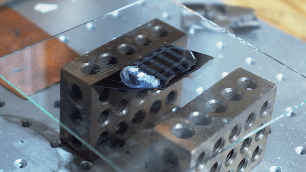
[Zachary Tong] is dipping his toes into the DIY semiconductor world, and further to the goal of keeping costs to a hobbyist scale, is experimenting with laser doping of silicon. Doping is the process of adding impurities to silicon wafers in a controlled manner to alter the electrical properties of the semiconductor. [Zach]’s doping method is a more localized version of the simple thermal diffusion method, which drives a dopant like phosphorus into silicon using high temperatures, but instead of using a tube furnace, he’s using a fiber laser.

The video below shows his two-step process, which first blasts the silicon oxide layer off the wafer before doping with the laser shining through a bath of phosphoric acid. The process is admittedly fussy, and the results were mixed at best. [Zach]’s testing seems to suggest that some doping occurred, and it even looks like he managed to make something reasonably diode-like using the method.

Although the jury is still out on [Zach]’s method, we thought the effort was the important bit here. Granted, not everyone has a fiber laser kicking around to replicate his results, but it’s always good to see progress in the DIY semiconductor field. Here’s hoping [Zach]’s work, along with the stuff that [Sam Zeloof] is doing, kicks off a spate of garage semiconductor fabs.

Continue reading “Laser Doping His Way To Homemade Silicon Chips”

Turing Ring Is Compact

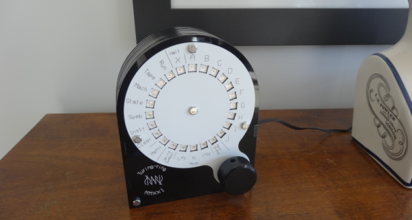
One of the problems with a classic Turing machine is the tape must be infinitely long. [Mark’s] Turing Ring still doesn’t have an infinite tape, but it does make it circular to save space. That along with a very clever and capable UI makes this one of the most usable Turing machines we’ve seen. You can see a demo in the video below.

The device uses an Arduino Nano, a Neopixel ring, an encoder, and a laser-cut enclosure that looks great. The minimal UI has several modes and the video below takes you through all of them.

Continue reading “Turing Ring Is Compact”