Ray's panels on the wall - circles of different sizes (from 60 to 15cm in diameter) covered by fabric of different shades, their arrangement vaguely resembling a cloud.

DIY Acoustic Panels Or Modern Artwork? Can’t Tell

The acoustic properties of a room have a surprising impact when you want to use a microphone. [RayP24]’s son was trying to make his bedroom into a better recording studio, and for [Ray], that turned into an artfully-executed wall panel project. Fortunately, the process is documented so we all can learn from it. When it comes to acoustics, you can often get a whole lot of improvement from surprisingly few changes. And, as this project demonstrates, you can make it look like a decorative piece to boot.

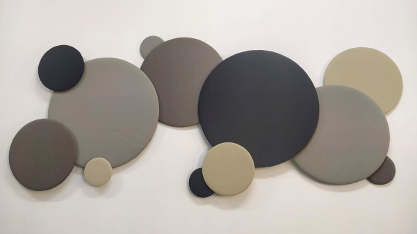
When arranged and placed on the wall, these panels look like an art piece, a decoration you could get from a somewhat fancy store. If you show them to someone, they might not believe that they also serve as a functioning home acoustics improvement, dampening the sound quite well for audio recording needs. The panels are built out of individual circles, cut out in a way that uses as much of a 3/16″ (5mm) plywood sheet as possible, with hollow circles serving as frames to attach foam-backed fabric. In the Instructables post, [Ray] talks quite a bit about how you can assemble your own and what liberties you can take. There’s also a short video accompanying this project, which you can see after the break. This project is begging to be recreated.

There’s a sizeable amount of hacking-meets-home improvement-meets-home acoustics projects out there, especially lately, when so many people are stuck at home for one reason or another. Just a few months ago, we covered another marvelous “art piece turned reverb killer” project operating by a slightly different principle, and also going a bit more into the theory. Perhaps in a few years, we will no longer have to build panels or structures for our soundproofing needs, as purpose-grown mycelium shapes will do that for us. And once it becomes a question of where to hang your newly-built acoustic panels, this simple guide is a good place to start.

Continue reading “DIY Acoustic Panels Or Modern Artwork? Can’t Tell”

Save Money And Have Fun Using IEEE-488

A few months ago, I was discussing the control of GPIB equipment with a colleague. Based on only on my gut feeling and the briefest of research, I told him that the pricey and proprietary GPIB controller solutions could easily be replaced by open-source tools and Linux. In the many weeks that followed, I almost abandoned my stance several times out of frustration. With some perseverance, breaking the problems into bite-sized chunks, and lots of online searching to learn from other people’s experiences, my plan eventually succeeded. I haven’t abandoned my original stance entirely, I’ve taken a few steps back and added some qualifiers.

What is GPIB?

Example of HP-IB block diagram from the 1970s, from hp9845.net

Back in the 1960s, if test equipment was interconnected at all, there weren’t any agreed-upon methods for doing so. By the late 60s, the situation was made somewhat better by card-cage controller systems. These held a number of interface cards, one per instrument, presenting a common interface on the backplane. Although this approach was workable, the HP engineers realized they could significantly improve the concept to include these “bridging circuit boards” within the instruments and replacing the card cage backplane with passive cables. Thus began the development of what became the Hewlett-Packard Interface Bus (HP-IB). The October 1972 issue of the HP Journal introduced HP-IB with two main articles: A Practical Interface System for Electronic Instruments and A Common Digital Interface for Programmable Instruments: The Evolution of a System. Continue reading “Save Money And Have Fun Using IEEE-488”

This Parametric Project Box Generator Is Super Easy

When it comes to taking an idea from concept to prototype reality, depending on the type of project, there can be quite a few sub-tasks along the way. Take for example, your latest electronic widget design. You’ve finished the schematic, and the PCB layout is a work of art (if you do say so yourself) but having that kicking around on the desk unprotected with wires dangling is not the end game. Now you’ve got to make an enclosure of some kind, and I don’t know about you, but this is the bit where this scribe struggles a little to get something to fit nice. Even if you’ve got the latest 3D printer dialed in to within a gnat’s whisker of perfection, you’ve still got to come up with the design, and those dimensions need to be really accurate. So, for those of us who are great at the PCB, but suck at the enclosure, [Willem Aandewiel] has been busy making the tool just for you, with his PCB-orientated Yet Another Parametric Projectbox generator (YAPP.)

Defining the PCB mounting points w.r.t. the PCB outline

Without hesitation you can head over to the YAPP GitHub, grab that sweet OpenSCAD code, and get cracking with the demos. Provided for your convenience are a number of examples for enclosing some common items, such as Arduinos and ESP32 modules, so you can use those as a springboard to get your own code in place. YAPP works based off the PCB — by specifying programmatically since this is OpenSCAD — outer dimensions, mounting post locations first. Next you define openings in the six faces of the box, and the tool happily spits out a platter with the base and lid ready to drop into Cura (or your slicer of choice) What could be easier?

End face cutouts

And before you start on non-rectangular designs, this is a rectangular box generator for rectangular PCBs. That is all this is designed for, and as far as we can tell, it does that one job well.

Of course, this is by no means the first enclosure generator to grace these pages, far from it. Here’s one for starters. If you’re here for tips to help make better designs, check this out, and finally 3DHubs also has a nice guide for you. Happy printing!

The decapped chip on top of some other DIP IC, with magnet wire soldered to the die, other ends of the magnet wire soldered to pins of the "body donor" DIP IC.

Factory Defect IC Revived With Sandpaper And Microsoldering

We might be amidst a chip shortage, but if you enjoy reverse-engineering, there’s never a shortage of intriguing old chips to dig into – and the 2513N 5×7 character ROM is one such chip. Amidst a long thread probing a few of these (Twitter, ThreadReader link), [TubeTime] has realized that two address lines were shorted inside of the package. A Twitter dopamine-fueled quest for truth has led him to try his hand at making the chip work anyway. Trying to clear the short with an external PSU led to a bond wire popping instead, as evidenced by the ESD diode connection disappearing.

A dozen minutes of sandpaper work resulted in the bare die exposed, making quick work of the bond wires as a side effect. Apparently, having the bond pads a bit too close has resulted in a factory defect where two of the pads merged together. No wonder the PSU wouldn’t take that on! Some X-acto work later, the short was cleared. But without the bond wires, how would [TubeTime] connect to it? This is where the work pictured comes in. Soldering to the remains of the bond wires has proven to be fruitful, reviving the chip enough to continue investigating, even if, it appears, it was never functional to begin with. The thread continued on with comparing ROMs from a few different chips [TubeTime] had on hand and inferences on what could’ve happened that led to this IC going out in the wild.

Such soldering experiments are always fun to try and pull off! We rarely see soldering on such a small scale, as thankfully, it’s not always needed, but it’s a joy to witness when someone does IC or PCB microsurgery to fix factory defects that render our devices inoperable before they were even shipped. Each time that a fellow hacker dares to grind the IC epoxy layers down and save a game console or an unidentified complex board, the world gets a little brighter. And if you aren’t forced to do it for repair reasons, you can always try it in an attempt to build the smallest NES in existence!

Continue reading “Factory Defect IC Revived With Sandpaper And Microsoldering”