Creating A PCB In Everything: KiCad, Part 1

This is the continuation of a series of articles demonstrating how to Create A PCB In Everything. In this series, we take a standard reference circuit and PCB layout — a simple ATtiny85 board — and build it with different PCB design tools. Already, we’ve taken a look at the pre-history of PCB design with Protel Autotrax, we learned Fritzing is a joke for PCB design, and we’ve done a deep dive into Eagle. Each of these tutorials serves two purposes. First, it is a very quick introduction to each PCB design tool. Second, this series provides an overall comparison between different PCB design tools.

Now, finally, and after many complaints, it’s time for the tutorial everyone has been waiting for. It’s time for KiCad.

No, like the head of the Bajoran clergy

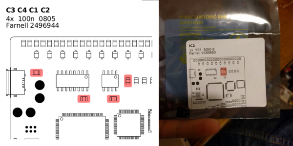
Although KiCad (pronounced ‘Kai-Cad’ like the head of the Bajoran clergy, not ‘Key-Cad’ like the thing that goes in a lock) is the new hotness when it comes to PCB design. The amazing growth of KiCad installations over the past few years is a long time coming. In development since 1992, KiCad has cemented itself as the premier Open Source PCB design suite, and since 2013 CERN has been making contributions to the project. More recently, the KiCad project has been showing off some amazing new features. These include 3D rendering of boards, interactive routing, push-and-shove, simulation, and dozens of other features that put it on a path to being on par with the top of the line EDA suites. Add in some great community contributions, and you have something really, really amazing. All of this is wrapped up in an Open Source license, free as in speech and beer. If you’re looking for the future of PCB design, Eagle is going to get very good but KiCad is almost there now while being Open Source.

Continue reading “Creating A PCB In Everything: KiCad, Part 1”

Hackenings: KiCAD, Science, DevOps, And Cyber

This week in [Hackenings], we’ve got a full roster of interesting upcoming events scattered all over the world. Can’t afford airfare to India, but Dublin is in the next county over? We’ve got you covered.

KiCad in Bangalore

IKP EDEN, in Bangalore, is hosting an Introduction to KiCad workshop on Sunday, Nov 13 from 10:00-2:00 pm. If you’re just getting started with PCB layout, or just want a quickstart learning KiCad, Hackaday contributor [Anool Mahidharia] will be there to show you how! Sign up on the link above, and bring your laptop with KiCad already installed.

Science in Dublin

20151115_124704-e1476655395528_thumbnailTOG hackerspace in Dublin is putting on their fifth annual Science Hack Day, a 36-hour hardware and software hackathon on Nov 19 & 20th. Looking through their photos, past creations have included a laser mission-impossible crawl-through maze thing, some kind of freaky turtle, and many objects that move, make noise, or otherwise amuse.

“Each year we bring together, designers, coders, scientists, engineers and makers. Simply to make interesting things. Why? For adventure, for playfulness, for science!”

DevOppery (and Foppery) in Stuttgart

logo_webDo you have what it takes to meet the needs of DevOps, Agile, and Cyber in the Enterprise Environment? Interested in Disruptive Cloud Computing or Mobile First Growth Hacking? Can you rub two buzzwords together and come up with marketing gold? Then you might have a fun time at the shack hackerspace in Stuttgart on Nov. 19th, for the eloop 2016 conference (translated here).

A full day’s talks include topics such as “Enterprise Patterns”, “Good Enough”, and the “Cult of Done Manifesto” as it relates to computer security. “What’s discussed at eloop today moves the digital markets of tomorrow.” YOLO!

Vote for Swindon

If you’re a UK citizen, you can vote to get the Swindon Makerspace some community funding so that they can furnish a new space. Why not?

Game Retro

And if you’re in Huntsville, Alabama, or environs, don’t forget Makers Local 256’s Retro Gaming night tonight (Saturday, 12th).

Hackenings? Hackenings!

[Hackenings] is our weekly Saturday morning (US, Pacific Time) roundup of what’s going to be going on in the hackerspace world in the upcoming week. If you’d like us to cover your event, email us at tips@hackaday.com and put [Hackenings] in the subject so that we don’t miss it. Thanks!

Scanning Parts Into KiCad

You do not know how to make a PCB unless you can make your own parts. [Jan] knows this, but like everyone else he checked out the usual online sources for a footprint for an SD card socket before making his own. It turns out, this SD card socket bought from an online marketplace was completely undocumented. Not only was an Eagle or KiCad footprint unavailable, but CAD files showing the dimensions of the part were non-existent. A solution had to be devised.

Instead of taking calipers and finely measuring all the pads on this SD card socket – a process that would surely fail – [Jan] decided to use a flatbed scanner to trace out the part. The part was placed on the glass and scanned at 300 dpi with a convenient reference object (a public transport card) in the same picture. This picture was imported into a CAD package, scaled to the correct ratio, and exported as a DXF. Since KiCad readily accepts importing DXFs, the CAD file was easily accessed, traced over, and a new part created.

From start to finish, making the footprint for this no-name, off-brand SD card socket took fifteen minutes. That’s nothing compared to the time it would take to manually measure each of the pads, draw a footprint, and print out the footprint at 1:1 scale to see if it matched up several times. It’s awesome work, and a great reminder that the best tools are usually right in front of you.

It’s Time To Finally Figure Out How To Use KiCAD

KiCAD has been making leaps and bounds recently, especially since CERN is using it almost exclusively. However, while many things are the same, just enough of them are different from our regular CAD packages that it’s hard to get started in the new suite.

[Chris Gammell] runs Contextual Electronics, an online apprenticeship program which goes from concept to assembled electronics covering everything in between. To take the course you pay a nominal fee, but [Chris] posted a very excellent ten-part video series made during the last run of classes which you can watch without charge. The videos go through the basics of KiCAD while hitting the major points to consider when designing and manufacturing your electronics.

The project [Chris] chose is a simple circuit that blinks an LED with a 555. The first videos cover navigating KiCAD’s component schematic editor and library system. Next comes creating circuit schematics and component footprint creation. [Chris] covers PCB layout, the generation of Gerber files, and finally ordering the design from OSH Park — the purveyors of purple boards we’ve come to know and love. The series finishes up with simulating the circuit in LTSpice, ordering the parts, and finally soldering and debugging of the board. If all goes correctly you should now have a single blinking LED.

If the bright summer sun is burning your delicate skin, and you’d rather be locked inside with solder fumes, add this to your watch list now!

Continue reading “It’s Time To Finally Figure Out How To Use KiCAD”

KiCAD BOM Management

KiCAD remains a popular tool for designing PCBs and other circuits, and with good reason: it’s versatile and it’s got pretty much everything needed to build any type of circuit board you’d want. It also comes with a pretty steep learning curve, though, and [Jeff] was especially frustrated with the bill of materials (BOM) features in KiCAD. After applying some Python and Kivy, [Jeff] now has a BOM manager that makes up for some of KiCAD’s shortcomings.

Currently, the tool handles schematic import, like-component consolidation, and a user-managed parts database that can be used to store and retrieve commonly used parts for the future. All of the changes can be saved back to the original schematic. [Jeff] hopes that his tool will save some time for anyone who makes more than one PCB a year and has to deal with the lack of BOM features native to KiCAD.

[Jeff] still has some features he’d like to add such as unit tests, a user guide, and a cleaner user interface. What other features are you anxious to see added to KiCAD?

This script is a great tool for anyone who has had similar frustrations. KiCAD is popular to modify and expand, too: there have been tools for mechanical CAD export, a parts-generator and cost-tracker, and an Eagle to KiCAD converter if you’re thinking of making the switch.

KiCad Traducido Al Español

KiCad ya es una gran herramienta para la captura esquemática y el diseño de PCB, pero el software sólo funciona si es posible utilizarlo. Para los mil millones de personas que no hablan inglés, esto significa que el idioma es la barrera más grande al momento de utilizar el mejor software para desarrollo de hardware. En los últimos meses, [ElektroQuark] ha estado liderando esfuerzos de localización al español de KiCad y estos se encuentran finalmente completados. También ha iniciado un foro de KiCad en idioma español para llevar el desarrollo de software hacia uno de los idiomas más hablado del planeta.

Spanish
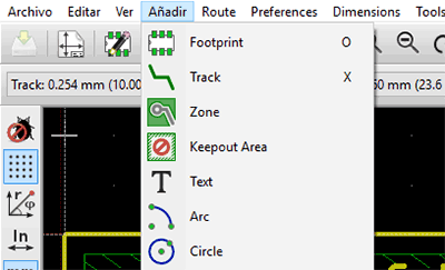
Mientras que ha habido otros intentos por localizar KiCad a otros idiomas, la mayoría de estos proyectos se encuentran incompletos. En una actualización de KiCad hace algunos meses, la localización al español ya contaba con algunas cadenas ya traducidas, pero no demasiadas. Los esfuerzos de [ElektroQuark] han acercado KiCad a millones de hablantes nativos de español, no solo algunos de sus menús.

El español es la segunda lengua más hablada del planeta, mientras que el inglés es la tercera. Teniendo en cuenta solamente este hecho, parece absurdo que casi todas las herramientas de software para capturas esquemáticas y diseño de PCB sean localizados sólo al chino o al inglés. Los esfuerzos de [ElektroQuark] por localizar KiCad al español son un gran avance para un ya impresionante software.

StickerBOM For KiCad

When boards were larger and components mostly through hole, designers could put a lot of information on the silk legend – reference designator, values, additional text and so on. But with surface mount components becoming smaller and board real estate at a premium, modern boards do not have a lot of information marked on the silk layer. If you are building and distributing a short run of kits, perhaps for a round of beta testing, then [Adam Greig]’s StickerBOM python script for KiCad can be really handy. StickerBOM is a KiCad BOM exporter designed for people stuffing boards by hand. It generates a PDF for printable sticky labels, where each label reflects one BOM line from a supplier. You then stick these labels on the bags from your supplier, and they show you where the parts go.

The labels get printed with the reference designator, quantity, component value, package, vendor and part number. It also adds a drawing of the PCB with the relevant parts highlighted for easy location identification. To use it, schematic symbols must have the supplier field and part number added. The script can be run from the command line, or from the BOM manager in eeschema. The script is set up for Avery L7164 labels, but this setting can be changed. It’s still work in progress so there’s a couple of bugs to be aware of. It cannot process the bottom layer of the board, and the result is only as good as the data you provide. And if you have a large board with components spread all over, the resultant graphic printed on the label may not be ideal.

We are hoping this, and other scripts such as the Part generator and Cost spreadsheets or the script for mechanical CAD export, get added to future releases of KiCad. The KiCad version 5 Developer’s road map document already has some really nice feature additions in the works.