Modernizing A Soviet-era LED Matrix

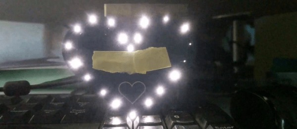
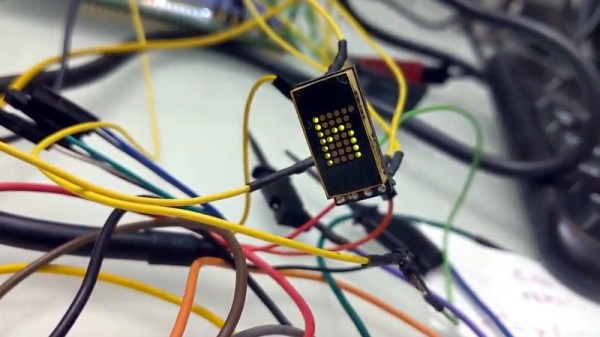
Used in everything from calculators to military hardware, the 3LS363A is an interesting piece of vintage hardware. With a resolution of 5 x 7 (plus a decimal point), the Soviet-made displays contain no electronics and are simply an array of 36 green LEDs. It’s not hard to drive one of them in a pinch, but [Dmitry Grinberg] thought this classic device deserved a bit better than the minimum.

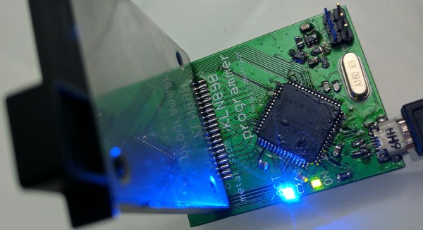
He’s developed a small board that sits behind the 3LS363A and allows you to control it over I2C for a much more modern experience when working with these vintage displays. Powered by the ATtiny406, his adapter board makes it easy to chain the modules together and even handles niceties like flipping the displayed image to account for different mounting positions. While most of us probably won’t have the chance to play around with these relatively rare displays, there’s still plenty of useful information here if you’re thinking of creating your own I2C gadgets.

In his write-up, [Dmitry] explains his rationale behind the design and some of the quirks of working with the display. For example he explains how he gave each column of the display its own FET, but to save space on the board ended up running the single decimal point (technically its own column) directly off of a spare GPIO pin. Relying on the low duty cycle, he even left current limiting resistors off the design. The end result is a tiny board that keeps the same footprint of the 3LS363A itself.

[Dmitry] went all out with developing the firmware for his new “smart” 3LS363A displays, and has written up documentation for the different commands he has implemented. From re-configuring the I2C address to updating the firmware, he’s made sure no stone was left unturned for this project. We’re not ones to shy away from a quick and dirty code, but it’s always nice to see when somebody has really put some thought into the software side of a project.

We’ve seen our fair share of oddball Soviet displays here at Hackaday, utilizing everything from heavy duty incandescent bulbs to remarkably tiny “intelligent” LEDs. While it’s unlikely any of them will dethrone the nixie as king of the retro display devices, it’s always interesting to see unusual hardware being used in the wild.

CortexProg Is A Real ARM-Twister

We’ve got a small box of microcontroller programmers on our desktop. AVR, PIC, and ARM, or at least the STMicro version of ARM. Why? Some program faster, some debug better, some have nicer cables, and others, well, we’re just sentimental about. Don’t judge.

[Dmitry Grinberg], on the other hand, is searching for the One Ring. Or at least the One Ring for ARM microcontrollers. You see, while all ARM chips have the same core, and thus the same SWD debugging interface, they all write to flash differently. So if you do ARM development with offerings from different chip vendors, you need to have a box full of programmers or shell out for an expensive J-Link. Until now.

[Dmitry] keeps his options open by loading up the flash-specific portion of the code as a plugin, which lets the programmer figure out what chip it’s dealing with and then lookup the appropriate block size and flash memory procedures. One Ring. He also implements a fast printf-style debugging aid that he calls “ZeroWire Trace” that we’d like to hear more about. Programming and debugging are scriptable in Lua, and it can do batch programming based on reading chip IDs.

You can build your own CortexProg from an ATtiny85, two diodes, and two current-limiting resistors: the standard V-USB setup. The downside of the DIY? Slow upload speed, but at least it’ll get you going. He’s also developed a number of fancier versions that improve on this. Version four of the hardware is just now up on Kickstarter, if you’re interested.

If you’re just using one vendor’s chips or don’t mind having a drawer full of programmers, you might also look into the Black Magic Probe. It embeds a GDB server in the debugger itself, which is both a cool trick and the reason that you have to re-flash the programmer to work with a different vendor’s chips. Since the BMP firmware is open, you can make your own for the cost of a sacrificial ST-Link clone, about $4.

On the other hand, if you want a programmer that works across chip families, is scriptable, and can do batch uploads, CortexProg looks like a caviar programmer on a fish-bait budget. We’re going to try one out soon.

Oh and if you think [Dmitry Grinberg] sounds familiar, you might like his sweet Dreamcast VRU hack, his investigations into the Cypress PSOCs, or his epic AVR-based Linux machine.

Write Your Own X86 Bootloader

What if you want to make a very lean machine and do without any operating system? Or maybe you want to try to write your own OS, even just for the challenge or fun? Maybe you were reading up on a cool OS architecture and thought to yourself, “I can write that!”. Well, before diving into your code, you’d first have to write something called a bootloader.

A bootloader is code that runs early on in a PC’s, Mac’s, Raspberry Pi’s or microcontroller’s boot sequence, before anything like an operating system is up. Often its job is to set up minimal hardware, such as RAM, and then load the OS or your embedded code.

[Alex Parker] has written a three-part series of clear blog posts that make writing the bootloader part easy, at least for x86 machines. And the nice thing is that you don’t need an x86 to get started. He does it on a Mac using the QEMU processor emulator, though he also talks about doing it under Windows and Linux.

In the first part of the series, the bootloader leaves you in the x86’s real mode, with 16-bit instructions and access to one megabyte of memory — think pre-80286 days, or 1982 for those of us who were computing back then. To prove it works, he uses BIOS calls to display “Hello world!”. This also shows that through the BIOS, you have a set of peripherals you can work with.

In the second part, he shows how to set up 32-bit protected mode and a Global Descriptor Table, making access to a large amount of memory easier.

In the first two parts, the code is written in assembly, so in the third part he finishes the series by showing how to load C++ code into memory and execute it. That C++ code would of course be your application, which we’ll leave to your imagination.

It’s reasonably rare to write bootloader code for a desktop computer — much less so for microcontrollers. For instance, [Dmitry Grinberg] wrote his own bootloader so that he could have encrypted ROM images for his AVR on USB. And we’ve talked about [Lady Ada]’s guide to burning Arduino bootloaders. But if you want to get down to the bare metal on your x86, the bootloader is the place to start. And it’s not so bad.

Completely Owning The Dreamcast Add-on You Never Had

If you’ve got a SEGA Dreamcast kicking around in a closet somewhere, and you still have the underutilized add-on Visual Memory Unit (VMU), you’re in for a treat today. If not, but you enjoy incredibly detailed hacks into the depths of slightly aged silicon, you’ll be even more excited. Because [Dmitry Grinberg] has a VMU hack that will awe you with its completeness. With all the bits in place, the hacking tally is a new MAME emulator, an IDA plugin, a never-before ROM dump, and an emulator for an ARM chip that doesn’t exist, running Flappy Bird. All in a month’s work!

The VMU was a Dreamcast add-on that primarily stored game data in its flash memory, but it also had a small LCD display, a D-pad, and inter-VMU communications functions. It also had room for a standalone game which could interact with the main Dreamcast games in limited ways. [Dmitry] wanted to see what else he could do with it. Basically everything.

We can’t do this hack justice in a short write-up, but the outline is that he starts out with the datasheet for the VMU’s CPU, and goes looking for interesting instructions. Then he started reverse engineering the ROM that comes with the SDK, which was only trivially obfuscated. Along the way, he wrote his own IDA plugin for the chip. Discovery of two ROP gadgets allowed him to dump the ROM to flash, where it could be easily read out. Those of you in the VMU community will appreciate the first-ever ROM dump.

On to doing something useful with the device! [Dmitry]’s definition of useful is to have it emulate a modern CPU so that it’s a lot easier to program for. Of course, nobody writes an emulator for modern hardware directly on obsolete hardware — you emulate the obsolete hardware on your laptop to get a debug environment first. So [Dmitry] ported the emulator for the VMU’s CPU that he found in MAME from C++ to C (for reasons that we understand) and customized it for the VMU’s hardware.

Within the emulated VMU, [Dmitry] then wrote the ARM Cortex emulator that it would soon run. But what ARM Cortex to emulate? The Cortex-M0 would have been good enough, but it lacked some instructions that [Dmitry] liked, so he ended up writing an emulator of the not-available-in-silicon Cortex-M23, which had the features he wanted. Load up the Cortex emulator in the VMU, and you can write games for it in C. [Dmitry] provides two demos, naturally: a Mandlebrot set grapher, and Flappy Bird.

Amazed? Yeah, we were as well. But then this is the same guy emulated an ARM chip on the AVR architecture, just to run Linux on an ATMega1284p.

Reading The Unreadable SROM: Inside The PSoC4

Wow. [Dmitry Grinberg] just broke into the SROM on Cypress’ PSoC 4 chips. The supervisory read-only memory (SROM) in question is a region of proprietary code that runs when the chip starts up, and in privileged mode. It’s exactly the kind of black box that’s a little bit creepy and a horribly useful target for hackers if the black box can be broken open. What’s inside? In the manual it says “The user has no access to read or modify the SROM code.” Nobody outside of Cypress knows. Until now.

This matters because the PSoC 4000 chips are among the cheapest ARM Cortex-M0 parts out there. Consequently they’re inside countless consumer devices. Among [Dmitry]’s other tricks, he’s figured out how to write into the SROM, which opens the door for creating an undetectable rootkit on the chip that runs out of each reset. That’s the scary part.

The cool parts are scattered throughout [Dmitry]’s long and detailed writeup. He also found that the chips that have 8 K of flash actually have 16 K, and access to the rest of the memory is enabled by setting a single bit. This works because flash is written using routines that live in SROM, rather than the usual hardware-level write-to-register-and-wait procedure that we’re accustomed to with other micros. Of course, because it’s all done in software, you can brick the flash too by writing the wrong checksums. [Dmitry] did that twice. Good thing the chips are inexpensive.

The nitty-gritty on the ROP (return oriented programming) tricks that [Dmitry] had to pull, and a good look into the design of the system itself, are all up on [Dmitry]’s blog. We can’t wait to see what other buried treasure he’s going to find as he continues to play around with these chips. And in case you’re wondering what type of mad genius it takes to pull this off, consider that [Dmitry] runs Linux on AVRs, fools nRF24 chips into transmitting Bluetooth LE beacons, and re-writes his own airplane’s GPS.

[Main image is a PSoC4200 dev kit, and [Dmitry] has only been working with the 4000 and 4100 series. Just so you know.]

Valentine’s Heart With Awesome Animations

January has drawn to a close, and for many of you that means: “Oh no! Less than two weeks’ time until Valentine’s day.” But for us here at Hackaday, it means heart-themed blinky projects. Hooray!

[Dmitry Grinberg] has weighed in with his version of the classic heart-shaped LED ring. It’s hard to beat the BOM on this one: just a microcontroller, five resistors, and twenty LEDs. The rest is code, and optionally putting the name of your beloved into the copper layer. Everything is there for you to download.

Continue reading “Valentine’s Heart With Awesome Animations”

KLN89B GPS data card reader/writer

Custom Data Writer Board For 1996 Plane’s GPS

[Dmitry Grinberg] recently bought a Cessna 150 that contained an old IFR-certified GPS from 1996, the KLN89B. The GPS unit contains a database which by law has to be kept up-to-date for IFR flight. The problem was that, while Honeywell still supplied the data in electronic form, [Dmitry] had no way to update the GPS. The original ways for doing it are either no longer supported, too expensive and a pain to do, or not available to him due to the way his GPS was installed.

Two of those ways involved removing a data card which can legally be slid out of the GPS’s front panel. The data card is what stores all the data but it’s a proprietary card and there’s no reader for it. [Dmitry]’s solution was therefore to make his own reader/writer board.

Continue reading “Custom Data Writer Board For 1996 Plane’s GPS”