Need A Thousand Extra PWM Pins?

If your Arduino runs out of I/O lines, you can always add one of the several I/O expander chips that takes a serial interface to set its several pins. Or perhaps you could buy something like an Arduino Mega, with its extra sockets to fulfil your needs. But what would you do if you really needed more pins, say a thousand of them? Perhaps [Brian Lough] has the answer. OK, full disclosure: If you really need a thousand, the video isn’t exactly for you, as he shows you how to add up to 992 PWM outputs. The chip he uses works with any microcontroller (the video shows an ESP8266), and we suppose you could use two daisy chains of them and break the 1,000 barrier handily.

We like how short the video is (just two minutes; see below) as it gets right to the point. The PCA9685 chip gives you 16 12-bit PWM channels via an I2C interface. You can daisy chain up to 62 of the boards to get the 992 outputs promised.

Continue reading “Need A Thousand Extra PWM Pins?”

Arrow’s $30 FPGA Board Reviewed

We like cheap FPGA boards. It isn’t just that we’re cheap — although that’s probably true, too — but cheap boards are a good way to get people started on FPGAs and we think more people should be using FPGAs more often. One inexpensive board is the Max-1000 from Trenz and Arrow. At $29, it is practically an impulse buy. [ZipCPU] did a great write up on his experience using the board. He found that some of it was good, some was bad, and some was just plain ugly. Still, for $30, it seems like this might be a nice board for some applications or for getting started.

Billed an IoT Maker Board, the tiny board sports a Intel (formerly Altera) MAX10 device with 8,000 logic elements, a USB programming interface onboard, 8 MB of SDRAM, and both PMOD and Arduino MKR headers. The MAX10 has an analog to digital conversion block (with an analog mux for up to nine channels) and the ability to host a 32-bit soft controller onboard, too.

Continue reading “Arrow’s $30 FPGA Board Reviewed”

34C3: Reverse Engineering FPGAs

We once knew a guy who used to tell us that the first ten times he flew in an airplane, he jumped out of it. It was his eleventh flight before he walked off the plane. [Mathias Lasser] has a similar story. Despite being one of the pair who decoded the iCE40 bitstream format a few years ago, he admits in his 34C3 talk that he never learned how to use FPGAs. His talk covers how he reverse engineered the iCE40 and the Xilinx 7 series devices.

If you are used to FPGAs in terms of Verilog and VHDL, [Mathias] will show you a whole new view of rows, columns, and tiles. Even if you don’t ever plan to work at that level, sometimes understanding hardware at the low level will inspire some insights that are harder to get at the abstraction level.

Continue reading “34C3: Reverse Engineering FPGAs”

An Open Source 96 MSPS Logic Analyzer For $22

If you are in the market for an inexpensive USB logic analyser you have a several choices, but few of them deliver much in the way of performance. There are kits from China for a few dollars using microcontrollers at their heart, but they fail to deliver significant sample rates. If you require more, you will have to pay for it.

It is therefore rather interesting to see [kevinhub88]’s SUMP2 project, an open source logic analyser with a claimed 96 MSPS sample rate using an off-the-shelf Lattice iCEstick FPGA evaluation board that only costs about $20. It talks to a host computer via USB using the established SUMP protocol, so its software front-end comes from the sump.org logic analyser project. Edit: Since this post was published [Kevin] has contacted us to inform us that the project’s capabilities have now moved beyond SUMP’s capabilities and in fact it now uses his own software.

This project has the promise to add a very useful piece of test equipment to the armoury of the engineer on a budget, and to aid the cost-conscious reader he’s provided extensive documentation and installation instructions, as well as the code for the FPGA. Thanks to one of the more awesome hacks of 2015, there is an entirely open toolchain for this Lattice part, and our own [Al Williams] has written up a multi-part getting-started guide if you want to get your feet wet. You probably want one of these anyway, and now it’s a logic analyzer to boot.

We’ve covered quite a few inexpensive home-produced digital instruments here over the years, including this logic analyser with a slightly higher price tag, this inexpensive VNA, and this oscilloscope board. Maybe one day the bench of our dreams will all come on one open-source PCB for $100, who knows!

Icestudio: An Open Source Graphical FPGA Tool

If you’ve ever worked with FPGAs, you’ve dealt with the massive IDEs provided by the vendors. Xilinx’s ISE takes about 6 gigabytes, and Altera’s Quartus clocks in at over 10 gigs. That’s a lot of downloading proprietary software just to make an LED blink.

[Jesús Arroyo]’s Icestudio is a new, graphical tool that lets you generate Verilog code from block diagrams and run it on the Lattice Semi iCEstick development board. A drag and drop interface lets you connect IOs, logic gates, dividers, and other elements. Once your block diagram is ready, a single button press downloads the code to the iCEstick.

Under the hood, Icestudio uses IceStorm, which we’ve discussed on HaD in the past, including this great talk by [Clifford], Icestorm’s lead. For the GUI, Icestudio uses nw.js, which spits out JSON based on the block diagram. This JSON is converted into a Verilog file and a PCF file. The Verilog is used to create the logic on the FPGA, and the PCF is used to define the pin configuration for the device. Clicking on selected modules reveals the generated Verilog if you want to know what’s actually going on.

It’s experimental, but this looks like a neat way to get started on FPGAs without learning a new language or downloading many gigs of toolchains. We’re hoping Icestudio continues to grow into a useful tool for education and FPGA development. A demo follows after the break.

[Thanks to Nils for the tip!]

Continue reading “Icestudio: An Open Source Graphical FPGA Tool”

Learning Verilog For FPGAs: The Tools And Building An Adder

Over the last year we’ve had several posts about the Lattice Semiconductor iCEstick which is shown below. The board looks like an overgrown USB stick with no case, but it is really an FPGA development board. The specs are modest and there is a limited amount of I/O, but the price (about $22, depending on where you shop) is right. I’ve wanted to do a Verilog walk through video series for awhile, and decided this would be the right target platform. You can experiment with a real FPGA without breaking the bank.

In reality, you can learn a lot about FPGAs without ever using real hardware. As you’ll see, a lot of FPGA development occurs with simulated FPGAs that run on your PC. But if you are like me, blinking a virtual LED just isn’t as exciting as making a real one glow. However, for the first two examples I cover you don’t need any hardware beyond your computer. If you want to get ready, you can order an iCEstick and maybe it’ll arrive before Part III of this series if published.

Continue reading “Learning Verilog For FPGAs: The Tools And Building An Adder”

Open Source FPGA Toolchain Builds CPU

When you develop software, you need some kind of toolchain. For example, to develop for an ARM processor, you need a suitable C compiler, a linker, a library, and a programmer. FPGAs use a similar set of tools. However, instead of converting source code to machine language, these tools map the intent of your source code into configuration of FPGA elements and the connections between them.

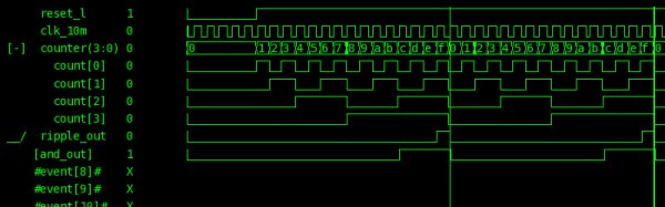
There’s some variation, but the basic flow in an FPGA build is to use a synthesizer to convert Verilog or VHDL to a physical design. Then a mapper maps that design to the physical elements available on a particular FPGA. Finally, a place and route step determines how to put those elements in a way that they can be interconnected. The final step is to generate a bitstream the chip understands and somehow loading it to the chip (usually via JTAG or by programming a chip or an external EEPROM).

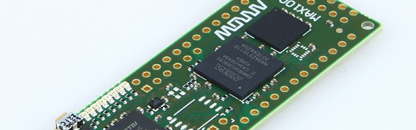
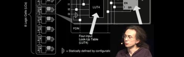
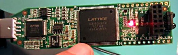
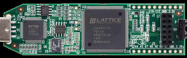
One problem with making your own tools is that the manufacturers typically hold the bitstream format and other essential details close to their chest. Of course, anything can be reverse engineered (with difficulty) and [James Bowman] was able to build a minimal CPU using  an open source Lattice toolchain. The project relies on several open source projects, including  IceStorm, which provides configuration tools for Lattice iCE40 FPGAs (there is a very inexpensive development platform available for this device).

We’ve covered IceStorm before. The IceStorm project provides three tools: one to produce the chip’s binary format from an ASCII representation (and the reverse conversion), a programmer for the iCEstick and HX8K development boards, and database that tells other open source tools about the device.

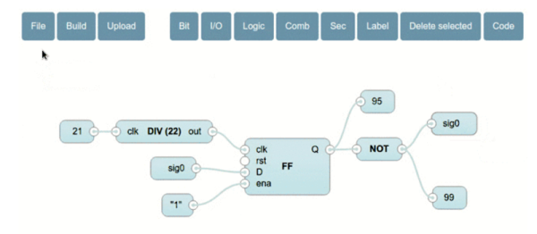
Those tools blend with other open source tools to form a complete toolchain–a great example of open source collaboration. Yosys does the synthesis (one of the tools available on the EDAPlayground site). The place and route is done by Arachne. The combined tools are now sufficient to build the J1A CPU and can even run a simple version of Forth. If you’ve ever wanted to play with an FPGA-based CPU design, you now have a $22 hardware option and free tools.

Continue reading “Open Source FPGA Toolchain Builds CPU”