FPGA Raises Component Video From A Sinclair ZX Spectrum

An abiding memory of the early-80s heyday of 8-bit computing for many is operating their computer from the carpet in front of the family TV. While the kids in the computer adverts had parents who bought them a portable colour telly on which to play Jet Set Willy, the average kid had used up all the Christmas present money on the computer itself. The cable would have been an RF connection to the TV antenna socket, and the picture quality? At the time we thought it was amazing because we didn’t know any different, but with the benefit of nearly 40 years’ hindsight, it was awful.

For ZX Spectrum owners in 2020 a standard modification is to bring out a composite video signal, but [c0pperdragon] has gone a step or two beyond that with a component video interface. And this isn’t a mod in which the signals are lifted from the Spectrum’s colour encoder circuitry, instead it uses an FPGA hooked directly to the ULA chip to generate the component video itself.

The Altera chip sits on a little PCB designed to occupy the footprint of the original Astec modulator, and sports a neat bundle of wires hooked up to the various Spectrum signals it needs. There are a couple of jumpers to select the output type and resolution, it supports YPbPr or RGsB outputs and both 288p and 576p. If you think perhaps it looks a little familiar, that’s because it’s the sister project of an earlier board for the Commodore 64. So if you have a Spectrum and are annoyed by UHF and PAL, perhaps it’s worth a look.

All Your Passwords Are Belong To FPGA

When used for cracking passwords, a modern high-end graphics card will absolutely chew through “classic” hashing algorithms like SHA-1 and SHA-2. When a single desktop machine can run through 50+ billion password combinations per second, even decent passwords can be guessed in a worryingly short amount of time. Luckily, advanced password hashing functions such as bcrypt are designed specifically to make these sort of brute-force attacks impractically slow.

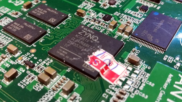
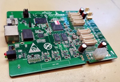
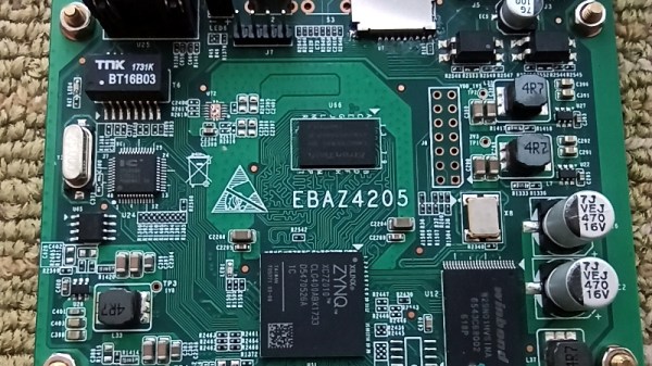
Cracking bcrypt on desktop hardware might be out of the question, but the folks over at [Scattered Secrets] had a hunch that an array of FPGAs might be up to the task. While the clock speed on these programmable chips might seem low compared to a modern CPUs and GPUs, they don’t have all that burdensome overhead to contend with. This makes the dedicated circuitry in the FPGA many times more efficient at performing the same task. Using a decade-old FPGA board intended for mining cryptocurrency, the team was able to demonstrate a four-fold performance improvement over the latest generation of GPUs.

An earlier version of the FPGA cracker

After seeing what a single quad FPGA board was capable of, the [Scattered Secrets] team started scaling the concept up. The first version of the hardware crammed a dozen of the ZTEX FPGA boards and a master control computer computer into a standard 4U server case. For the second version, they bumped that up to 18 boards for a total of 72 FPGAs, and made incremental improvements to the power and connectivity systems.

Each 4U FPGA cracker is capable of 2.1 million bcrypt hashes per second, while consuming just 585 watts. To put that into perspective, [Scattered Secrets] says you’d need at least 75 Nvidia RTX-2080Ti graphics cards to match that performance. Such an array would not only take up a whole server rack, but would burn through a staggering 25 kilowatts. Now might be a good time to change your password to something longer, or finally get onboard with 2FA.

We’ve covered attempts to reverse engineer hardware designed for cryptocurrency mining, but those were based around application-specific integrated circuits (ASICs) which by definition are very difficult to repurpose. On the other hand, disused FPGA-based miners offer tantalizing possibilities; once you wrap your mind around how they work, anyway.

[Thanks to Piejoe for the tip.]

Crunching Giant Data From The Large Hadron Collider

Modern physics experiments are often complex, ambitious, and costly. The times where scientific progress could be made by conducting a small tabletop experiment in your lab are mostly over. Especially, in fields like astrophysics or particle physics, you need huge telescopes, expensive satellite missions, or giant colliders run by international collaborations with hundreds or thousands of participants. To drive this point home: the largest machine ever built by humankind is the Large Hadron Collider (LHC). You won’t be surprised to hear that even just managing the data it produces is a super-sized task.

Since its start in 2008, the LHC at CERN has received several upgrades to stay at the cutting edge of technology. Currently, the machine is in its second long shutdown and being prepared to restart in May 2021. One of the improvements of Run 3 will be to deliver particle collisions at a higher rate, quantified by the so-called luminosity. This enables experiments to gather more statistics and to better study rare processes. At the end of 2024, the LHC will be upgraded to the High-Luminosity LHC which will deliver an increased luminosity by up to a factor of 10 beyond the LHC’s original design value.

Currently, the major experiments ALICE, ATLAS, CMS, and LHCb are preparing themselves to cope with the expected data rates in the range of Terabytes per second. It is a perfect time to look into more detail at the data acquisition, storage, and analysis of modern high-energy physics experiments. Continue reading “Crunching Giant Data From The Large Hadron Collider”

The DOOM Chip

It’s a trope among thriller writers; the three-word apocalyptic title. An innocuous item with the power to release unimaginable disaster, which of course our plucky hero must secure to save the day. Happily [Sylvain Lefebvre]’s DOOM chip will not cause the world to end, but it does present a vision of a very 1990s apocalypse. It’s a hardware-only implementation of the first level from id Software’s iconic 1993 first-person-shooter, DOOM. As he puts it: “Algorithm is burned into wires, LUTs and flip-flops on an #FPGA: no CPU, no opcodes, no instruction counter. Running on Altera CycloneV + SDRAM”. It’s the game, or at least the E1M1 map from it sans monsters, solely in silicon. In a very on-theme touch, the rendering engine has 666 lines of code, and the level data is transcribed from the original into hardware tables by a LUA script. It doesn’t appear to be in his GitHub account so far, but we live in hope that one day he’ll put it up.

“Will it run DOOM” is almost a standard for new hardware, but it conceals the immense legacy of this game. It wasn’t the first to adopt a 1st-person 3D gaming environment, but it was the game that defined the genre of realistic and immersive FPS releases that continue to this day. We first played DOOM on a creaking 386, we’ve seen it on all kinds of hardware since, and like very few other games of its age it’s still receiving active development from a large community today. We still mourn slightly that it’s taken the best part of three decades for someone to do a decent Amiga port.

Using An FPGA To Glitch The Olimex LPC-P1343

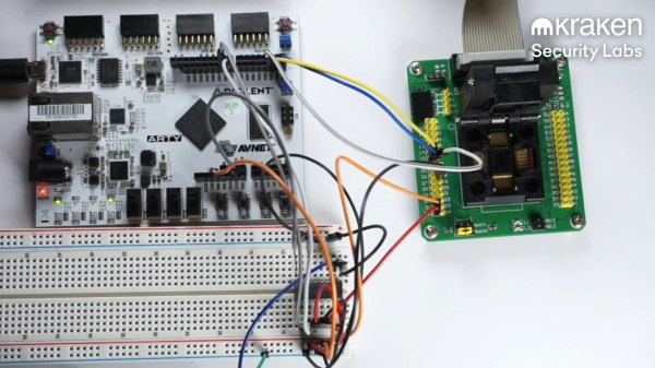
After trying out hardware hacking using an FPGA to interface with target hardware, [Grazfather] was inspired to try using the iCEBreaker (one of the many hobbyist FPGAs to have recently flooded the market) to build a UART-controllable glitcher for the Olimex LPC-P1343.

FPGA Modules (The cmd module intercepts what the host computer sends over UART, the resetter holds the reset line until the target is reset, the delay starts counting on reset and waits for a configured number of cycles before sending its signal, the trigger waits for the delay to finish before telling the pulse module to send a pulse, and the pulse works similar to the delay module and outputs to the power multiplexer.)

When the target board boots up, the bootROM reads the flash and determines whether the UART goes to a shell and if the shell can be used to read out the flash. This is meant for developing firmware and debugging it in the bootloader, only flashing a version when the firmware is production-ready. The vulnerability is that only a specific value read from address 0x2FC and the state of a few pins can lock the bootloader in the expected way, and any other value at the address causes the bootROM to consider the device unlocked. Essentially, the mechanism is the opposite of how a lock ought to work.

The goal is to get the CPU to misread the flash at the precise moment it is meant to be reading the specific value, then jumping to the bootloader in the unlocked state. The FPGA can be used as a tool between the host machine and target board, communicating via UART. The FGPA can support configuring the delay between resetting the target board and pulsing a ‘glitch voltage’, as well as resetting the target board and activating the glitch. The primary reasons for using the FPGA over a different microcontroller are that the FPGA allows for precise timing (83.3ns precision) and removes worries about jitters (a Raspberry Pi might have side effects from OS scheduling and other processes and microcontrollers might have interrupts messing up the timing).

The logic analyzer view

To simulate the various modules, [Grazfather] used Icarus Verilog as well as GTKWave to observe the waveforms generated. A separate logic analyzer observes the effects on real hardware.

With enough time, it is possible to brute force any combination of delay and width until you get a dump of the flash you’re not meant to read. You can check out how the width of the pulse gets wider until the max, when the delay is incremented and the width values are tried again.

Continue reading “Using An FPGA To Glitch The Olimex LPC-P1343”

NEO430 Puts A Custom MSP430 Core In Your FPGA

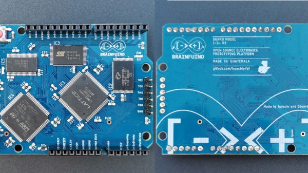
We are certainly spoiled by all the microcontroller options nowadays — which is a great problem to have. But between the good old 8-bit controllers and an increasing number of 32-bit varieties, it almost seems as if the 16-bit ones are slowly falling into oblivion. [stnolting] particularly saw an issue with the lack of 16-bit open source soft cores, and as a result created the NEO430, an MSP430 compatible soft processor written in VHDL that adds a custom microcontroller to your next FPGA project.

With high customization as main principle in mind, [stnolting] included a wide selection of peripherals and system features that can be synthesized as needed. Not limiting himself to the ones you would find in an off-the-shelf MSP430 controller, he demonstrates the true strength of open source soft cores. Do you need a random number generator, CRC calculation, and an SPI master with six dedicated chip select lines? No problem! He even includes a Custom Functions Unit that lets you add your own peripheral feature or processor extension.

However, what impresses most is all the work and care [stnolting] put into everything beyond the core implementation. From the C library and the collection of examples for each of the controller’s features, so you can get started out of the box with GCC’s MSP430 port, to writing a full-blown data sheet, and even setting up continuous integration for the entire repository. Each topic on its own is worth looking at, and the NEO430 offers a great introduction or reference for it.

Of course, there are some shortcomings as well, and the biggest downer is probably the lack of analog components, but that’s understandable considering your average FPGA’s building blocks. And well, it’s hard to compete with the MSP430’s ultra low-power design using an FPGA, so if you’re thinking of replicating this watch, you might be better off with a regular MSP430 from a battery lifetime point of view.

Researchers Break FPGA Encryption Using FPGA Encryption

FPGAs are awesome — they can be essentially configured into becoming any computing device you want. Simply load your selected bitstream into the device on boot, and it behaves like a different piece of hardware. With great power comes great responsibility.

You might try to hack a given FPGA system by getting between the EEPROM that stores the bitstream and the FPGA during bootup, but FPGA manufacturers are a step ahead of you. Xilinx 7 series FPGAs have an onboard encryption and signing engine, and facilities for storing a secret key. Once the security bit is set, bitstreams coming in have to be encrypted to protect from eavesdropping, and HMAC-signed to assure that they are authentic. You can’t simply read the bitstream in transit or inject your own.

Researchers at Ruhr University Bochum and Max Planck Institute for Cybersecurity and Privacy in Germany have figured out a way to use the FPGA’s own encryption engine against itself to break both of these security guarantees for the entire mainstream 7-series. The attack abuses a MultiBoot function that allows you to specify an address to begin execution after reboot. The researchers send 32 bits of the encoded payload as a MultiBoot address, the FPGA decrypts it and stores it in a register, and then resets because their command wasn’t correctly HMAC signed. But because the WBSTAR register is meant to be readable on boot after reset, the payload is still there in its decrypted form. Repeat for every 32 bits in the bitstream, and you’re done.

Pulling off this attack requires physical access to the FPGA’s debug pins and up to 12 hours, so you only have to worry about particularly dedicated adversaries, but the results are catastrophic — if you can reconfigure an FPGA, you can make it do essentially anything. Security-sensitive folks, we have three words of consolation for you: “restrict physical access”.

What does this mean for Hackaday? If you’re looking at a piece of hardware with a hardened Xilinx 7-series FPGA in it, you’ll be able to use it, although it’s horribly awkward for debugging due to the multi-hour encryption procedure. Anyone know of a good side-channel bootloader for these chips? On the other hand, if you’re just looking to dig secrets out from the bitstream, this is a one-time cost.

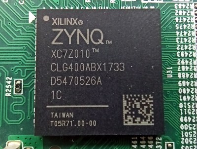
This hack is probably only tangentially relevant to the Symbiflow team’s effort to reverse-engineer an open-source toolchain for this series of FPGAs. They are using unencrypted bitstreams for all of their research, naturally, and are almost done anyway. Still, it widens the range of applicability just a little bit, and we’re all for that.

[Banner image is a Numato Lab Neso, and comes totally unlocked naturally.]