The Field Programmable Gate Array (FPGA) is one of the most exciting tools in the modern hacker’s arsenal. If you can master the FPGA, you can create hardware devices that not only morph and change based on your current needs, but can power through repetitive tasks at phenomenal rates. The only problem is, working with FPGAs can be a bit intimidating for newbies. One could argue that the technology is waiting on its “Arduino” moment; the introduction of a cheap development board coupled with easy to use software that brings FPGA hacking into the mainstream.
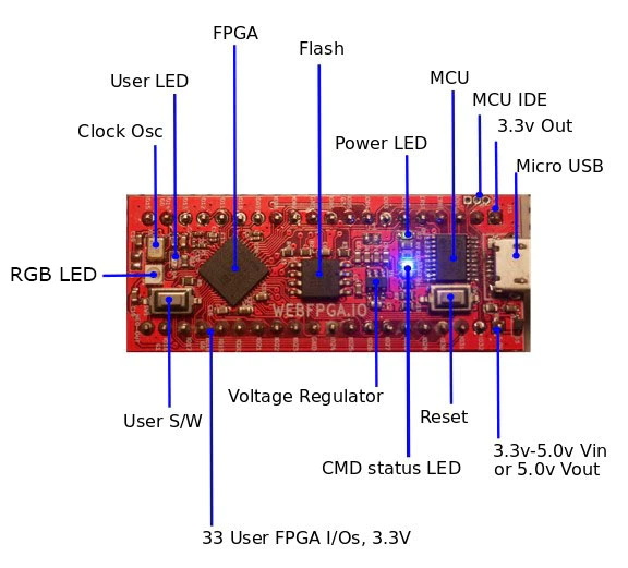 If everything goes according to plan, the wait might soon be over. [Ryan Jacobs] believes his project WebFPGA is the easiest and fastest way to get your hands dirty with this incredible technology. Outwardly the hardware could pass for an Arduino Nano clone, with a bunch of GPIO pins and a couple of LEDs on a small breadboard-friendly PCB. Certainly a no-frills presentation. It’s the software side is where things get interesting: all you need to develop for this FPGA is a modern web browser.
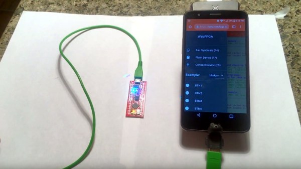
Currently Chrome, Opera, and Edge are supported, even if they’re running on relatively low-end computers. [Ryan] says this makes it much easier and cheaper to roll out FPGA classes in schools, as students can do everything with their existing Chromebooks. As the video after the break shows, you can even get away with using a sufficiently powerful smartphone to do some FPGA hacking on the go.
So what’s the trick? Essentially the heavy-lifting is done remotely: all of the synthesis is performed in their cloud backend, with the final bitstream delivered to the user for installation through WebUSB. If you’re more comfortable on the command line, [Ryan] says they’re currently working on tools which will allow you to perform all the necessary interactions with their cloud service without the browser.
The more critical Hackaday reader will likely be concerned about lock-in. What happens if you buy one of these development boards without a license for the service, or worse, what happens if WebFPGA goes belly-up down the road? To that end, [Ryan] makes it clear that their hardware is completely compatible with existing offline FPGA development tools such as the open source IceStorm.
We’ve seen considerable interest in low-cost FPGA development platforms, with readers perhaps recalling the excitement surrounding the fire sale of the Pano Logic thin clients. Despite efforts to make developing for these systems even easier, it’s hard to imagine the bar getting much lower than what WebFPGA is shooting for. Their Kickstarter campaign is close to crossing the finish line, and we’re very interested to see where the product goes from here.