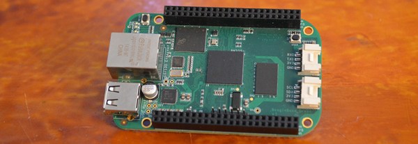
Although the BeagleBone Green was announced at the Bay Area Maker Faire last May, there hasn’t been much said about it on the usual forums and IRC channels. Now, it’s finally out and I got my hands on one of them. Through a cooperation between the BeagleBoard foundation and Seeed Studios, the best small Linux board for doing real work with small Linux boards is now cheaper, a little more modern, and green.
The BeagleBone Green is an update to the venerable BeagleBone Black, the dev board based on a TI ARM Cortex-A8. It’s an extremely capable machine with a few interesting features that make it the perfect device for embedded applications. With the BeagleBone Green, the BB Black gets a small hardware refresh and a drastic reduction in price. If you want to do real work on a Linux board, this is the one to get. Check out the review below for everything that’s been updated, everything that’s the same, and why this is one of the most interesting developments in small Linux boards in recent memory.
Auto site [Jalopnik] got some hands-on (or rather feet-on) time with the Lexus hoverboard that was built for an advert for the luxury car brand, and their video reveals a few secrets about how this interesting device works. It is definitely real: the Jalopnik writer got to ride it himself, and described it as “Unbelievably difficult yet at the same time unbelievably cool, both because you’re levitating and because the board is filled with magnets more than 300 degrees below zero“. But a look behind the scenes reveals that it is another tease.
The device looks like it is a real hoverboard, floating several inches above the surface and even traveling over water, a feat that Marty McFly couldn’t do. But, as usual, there is a little more going on than meets the eye. The device is built around superconducting magnets cooled by liquid nitrogen, so it only works for about 10 minutes. After that, you have to refill the device with liquid nitrogen. The surface that the board is floating over also has what the Jalopnik writer describes as having “several hundred thousand dollars worth of magnets built in“. Try this on a non-magnetic surface and you’ll come to a grinding halt. If you watch the video of the hoverboard serenely gliding over the water from another angle, you can see a magnetic track just under the surface. If you run off this track, you’ll end up with wet feet.
Is it a neat hack? Yes. Is it cool? Yes. Is it the future of transportation? No: it is a cool hack put together for a car advert with a big budget. Kudos to Lexus for spending the cash to do it properly, but once again, our dreams of hoverboards are dashed in the cold, hard light of reality. Darn.
CMOS opened the door for many if not most of the properties needed for today’s highly integrated circuits and low power portable and mobile devices. This really couldn’t happen until the speeds and current drive capabilities of CMOS caught up to the other technologies, but catch up they did.
Nowadays CMOS Small Scale Integration (SSI) logic families, I.E. the gates used in external logic, offer very fast speeds and high current drive capability as well as supporting the low voltages found in modern designs. Likewise the Very Large Scale Integration (VLSI) designs, or Very Very Large Scale if you like counting the letter V when talking, are possible due to low power dissipation as well as other factors.
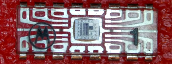
Microchips and integrated circuits are usually treated as black boxes; a signal goes in, and a signal goes out, and everything between those two events can be predicted and accurately modeled from a datasheet. Of course, the reality is much more complex, as any picture of a decapped IC will tell you.
The four transparent chips are beautiful works of engineering art, with the chip carriers, the bond wires, and the tiny square of silicon all visible to the naked eye. The educational set covers everything from resistors, n-channel and p-channel MOSFETS, diodes, and a ring oscillator circuit.
[Jim] has the chips and the datasheets, but doesn’t have the teaching materials and lab books that also came as a kit. In lieu of proper pedagogical technique, [Jim] ended up doing what any of us would: looking at it with a microscope and poking it with a multimeter and oscilloscope.
While the video below only goes over the first chip packed full of resistors, there are some interesting tidbits. One of the last experiments for this chip includes a hall effect sensor, in this case just a large, square resistor with multiple contacts around the perimeter. When a magnetic field is applied, some of the electrons are deflected, and with a careful experimental setup this magnetic field can be detected on an oscilloscope.
[Jim]’s video is a wonderful introduction to the black box of integrated circuits, but the existence of clear ICs leaves us wondering why these aren’t being made now. It’s too much to ask for Motorola to do a new run of these extremely educational chips, but why these chips are relegated to a closet in an engineering lab or the rare eBay auction is anyone’s guess.
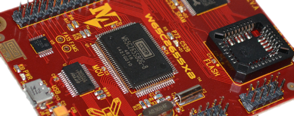
The 6502 is a classic piece of computing history. Versions of this CPU were found in everything from the Apple ][, to the Nintendo Entertainment System, and the Commodore 64. The history of the 6502 doesn’t end with video games; for the last forty years, this CPU has found its way into industrial equipment, medical devices, and everything else that doesn’t need to be redesigned every two years. Combine the longevity of the 6502 with the fact an entire generation of developers first cut their teeth on 6502 assembly, and you have the makings of a classic microprocessor that will, I’m sure, still be relevant in another forty years.
The folks at WDC recently contacted me to see if I would give their hardware a close look, and after providing a few boards, this hardware proved to be both excellent. They’re great for educators adventurous enough to deviate from the Arduino, Processing, and Fritzing zeitgeist, and for anyone who wants to dip their toes into the world of 65xx development.
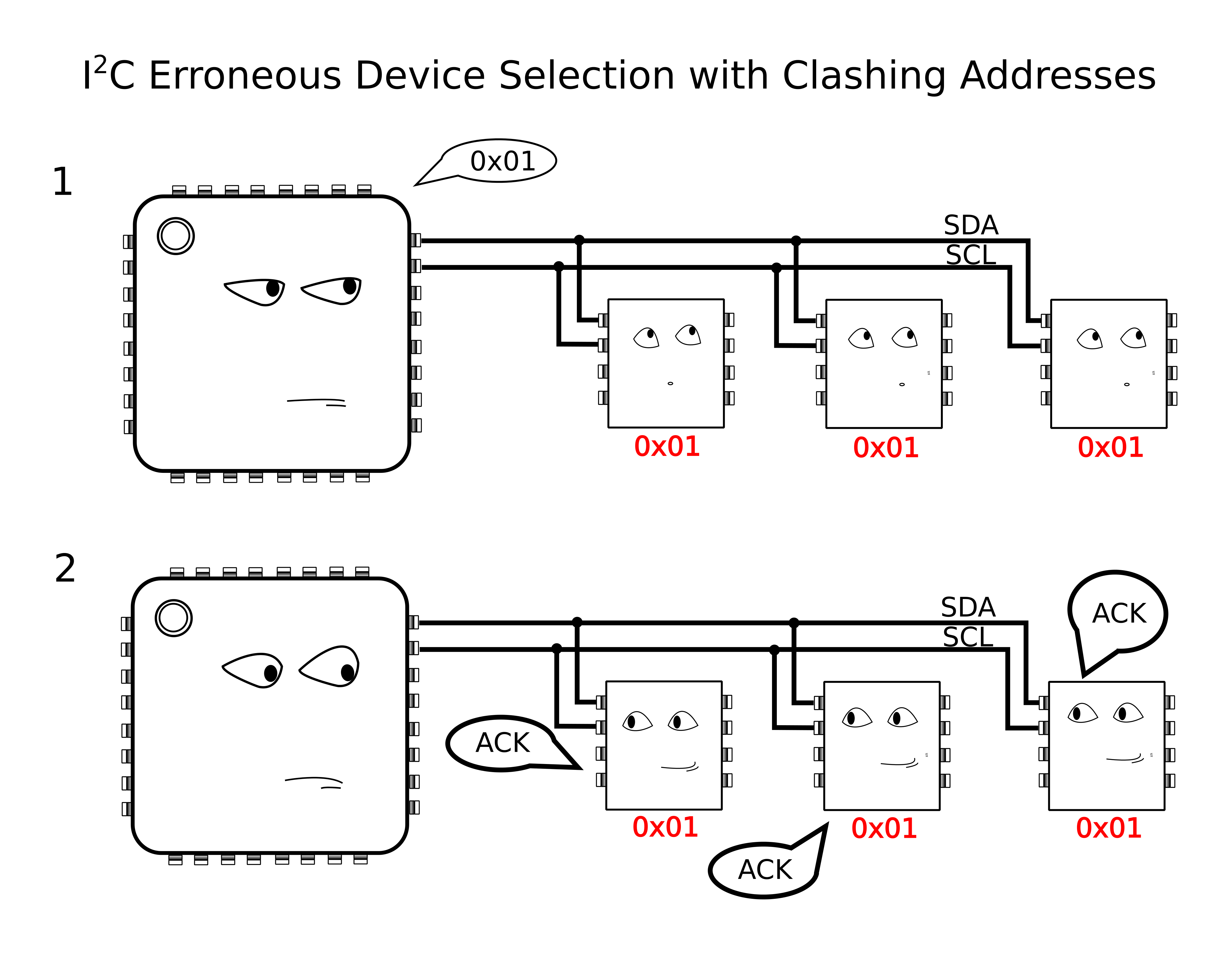
There comes a time when you need to wire up three, four, or more identical i2c devices to a common microcontroller. Maybe you’re thinking about driving 128 seven-segment displays with eight of those MAX6955 16-way digit drivers, or maybe you have a robot full of joints–each of which needs a BNO055 inertial sensor for angle estimation. (See above.) Crikey! In both of those cases, you’re best bet might be a schnazzy I²C device that can do most of the work for you. The problem? With a single I²C bus, there’s no standard way defined in the protocol for connecting two or more devices with the same address. Shoot! It would’ve been handy to wire up three BNO055 IMUs or eight MAX6955s and call it a day. Luckily, there’s a workaround.
We’ve seen some clever tricks in the past for solving this problem. [Marv G‘s] method involves toggling between a device’s default and alternate address with an external pin. This method, while clever, assumes that the device (a) has an alternate I²C address and (b) features an external pin for toggling that address.
I’ll introduce two additional methods for getting the conversation started between your micro’ and your suite of identical sensors. The first is “a neat trick,” but somewhat impractical for widespread use. The second is far more production-worthy–something you could gloat over and show off to your boss! Without further ado, let’s get started with Method 1.
Lastly, if you’d like to follow along, feel free to check out the source code on Github.
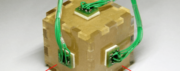
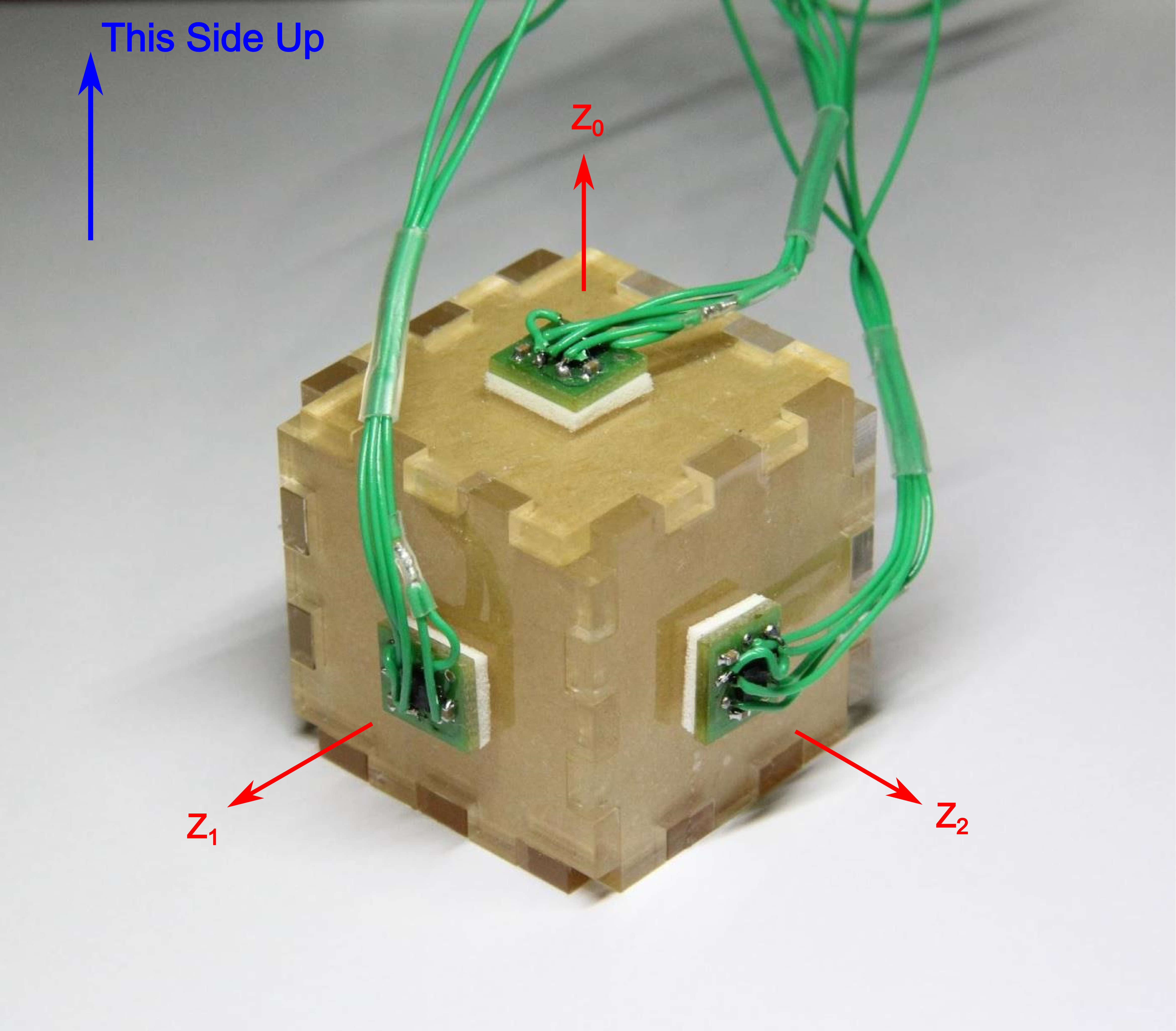
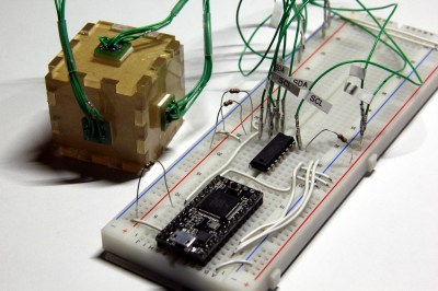
In both methods, I’m using the same sensor setup to check that each circuit behaves correctly. I happened to have a bunch of extra BMA180s on the bench, so I rolled out an example based on these chips. Back in the day, the BMA180 was a pretty common three-axis digital accelerometer. It has an I²C interface with two optional addresses. For the purpose of this example, I’m fixing them all with the same address. I’ve mounted three of these guys on mutually perpendicular axes of my acrylic “test cube,” and I’m reading each chip’s Z-axis. In this configuration I can easily pick out the gravity vector from the corresponding sensor as the data goes flying by my serial port window. If I can uniquely address each sensor and read the data, I’ve got a working circuit.
Method 1: Splicing Clocks into Chip-Selects
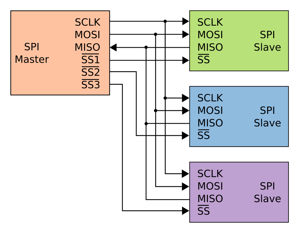
This method tips its hat towards SPI in that it behaves in an oddly similar fashion. If you’re feeling rusty on SPI, here’s a quick recap.
A Quick SPI Refreshment:
SPI, like I²C, is another protocol that shares both its clock and data lines with multiple slave devices. The difference, though, lies in the addressing scheme to talk to these devices that share the same bus. With SPI, while clock and data lines are shared, devices are addressed with separate chip-select (CS) lines.
The master microcontroller dedicates a unique output pin to each device (~SS1, ~SS2, and ~SS3 in this illustration). When the master micro’ wants to talk to a device, it asserts that device’s chip-select input pin by pulling it to logic LOW, and the conversation begins over the data bus. With the chip select LOW, the corresponding slave listens to the data on the bus. Meanwhile, all other devices ignore the conversation between the master and it’s chosen slave by keeping their bus pins in a high impedance state.
Giving I²C Its Own Chip-Selects:
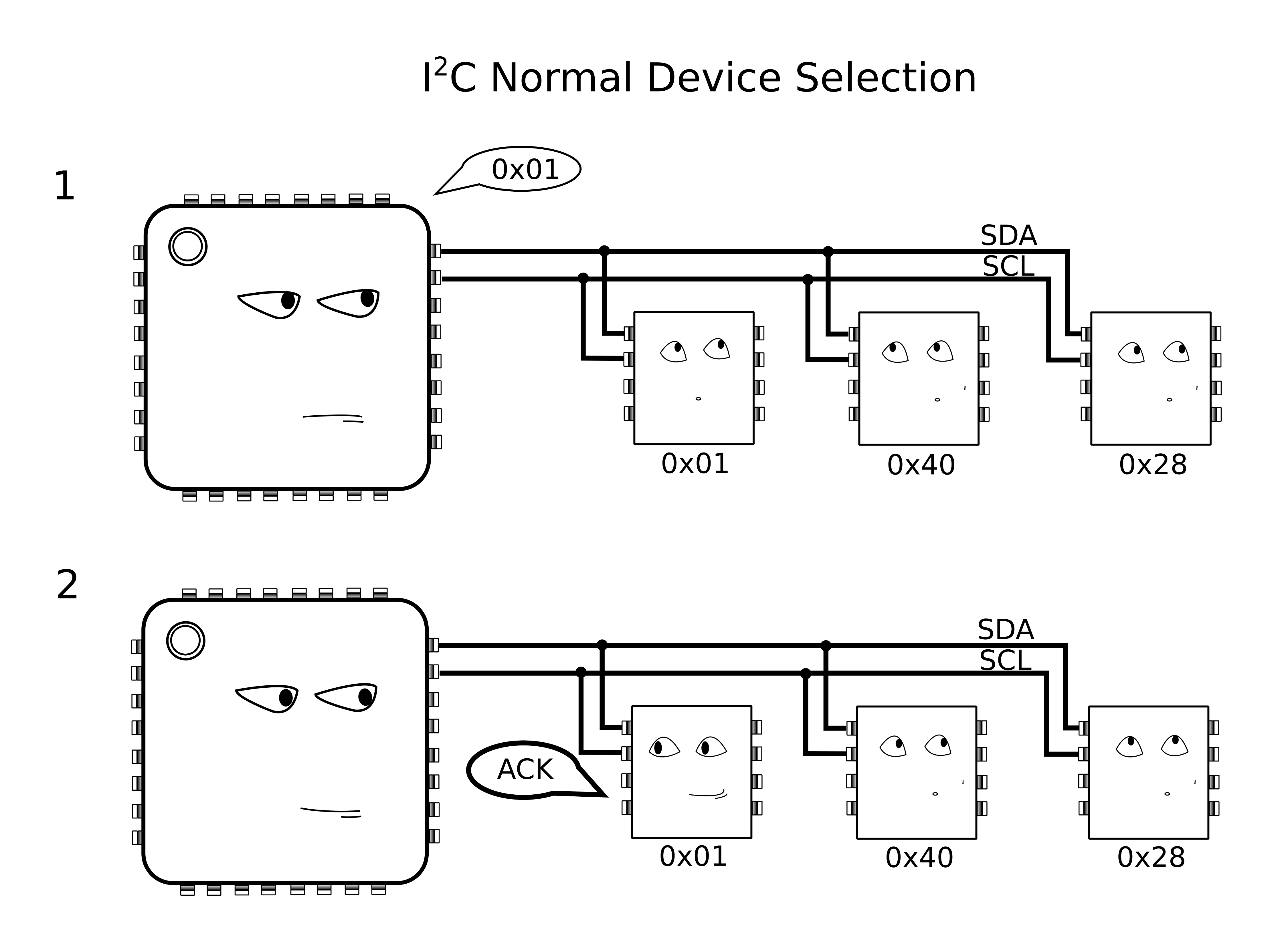
With I²C, Clock (SCL) and Data (SDA) lines are still shared between all I2C slave devices, but the addressing scheme happens by sending a message heard by all devices on the bus. To single out one device on the shared bus, the master first passes down the address of the slave device it wants to talk to, after which that slave replies with an ACKnowledge, and all other slaves ignore the data that follows until both data transmission is complete and the bus is “released.”
Because we have the problem of multiple devices with shared addresses, in theory, all of these devices would reply when the master passes down their shared address, and there’s no way for the master to single out a single device. In reality, this behavior is undefined on the I²C protocol.
Yikes! Anything goes when we wander away from defined behavior, so we try to avoid these things in practice.
The solution?
According to the I²C spec, It just so happens that an I²C slave device will ignore changes on the data line (SDA) provided that the clock line (SCL) is held high. In this method, I’ll “split” the SCL line into multiple SCL lines such that each shared I²C device gets its own SCL. By selectively rerouting the clock to each I²C device one-at-a-time, I’ve essentially turned the SCL line into a “chip select.”
To chop up that clock line, I’ll need a demultiplexer. A demultiplexer (or decoder) takes a logical input and reroutes it to one of several outputs based on the binary select lines.
I’ve dropped in the 74AC11138 eight-way demultiplexer for this task. It’s fast, capable of switching at megahertz rates, and its outputs default to logic HIGH. That second note is handy since idle SCL lines also default to logic HIGH.
The setup is shown in a simplified schematic above. In it, I’m using a Teensy 3.0 posing as the I²C bus master. To the right of the Teensy is the collection of identical chips, BMA180 accelerometers in this case. In the middle is the 74AC11138 eight-way demultiplexer.
Cons of this Method:
There’s a minor drawback with this technique, though, in that it doesn’t support I²C’s clock-stretching feature. Taking a step back, this method assumes that the SCL line is inherently unidirectional, controlled by only the I²C bus master. In other words, we’re making the assumption that data on the SCL line is only sent from master to slave and never the other way around. If your I²C slave devices implement clock-stretching, however, this assumption breaks down.
What is Clock Stretching?
Clock stretching is a method defined by the I²C protocol where the chip needs to “buy itself more time” and holds the SCL line low, hence, signalling to the master that it’s not ready for the upcoming data. In this scenario, the slave actively controls the SCL line, and it happens to be the only case where data moves up the SCL line from slave to master. In a setup with our demultiplexer between the master and our set of identical slaves, these slaves won’t be able to send back the clock-stretching signal to the master to indicate that they aren’t ready for data, if they happen to implement clock stretching. That said, clock stretching is a pretty rare feature among I²C-compatible devices, so this method is likely to work among a number of chips out now.
More Next Week
That’s all for Method 1. Thanks for tuning in, and check back next week for a slightly-more-professional method of tackling this same problem.
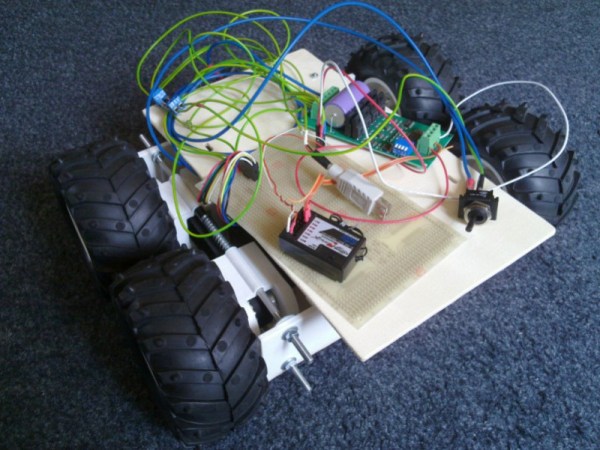
[Andrey Nechypurenko] has posted the second part of his robotics ground vehicle design guide. In his first post [Andrey] detailed the mechanical design decisions he faced. [Andrey] now begins covering the electrical components, starting with manual control using a standard radio control system. To accomplish this an RC system was used with an MD22 h-bridge driver and a picoUPS.
The MD22 is a neat motor control board which can take the PWM signals from the radio controller and use this to drive the DC motors. Optionally it can also use an I2C interface, giving a nice migration path to integrate with a microcontroller. Until that happens this can’t really be called a robot — its more of an RC vehicle. But the iterative design and build process he’s using is a good one!
The picoUPS provides on-board battery charging. Due to its UPS heritage it also allows the vehicle to be powered from an external supply, which has proved useful during development. Finally, a 5v regulator was required to supply the on-board digital logic. [Andrey] wanted a quick drop in solution with a budget large enough to allow for future expansion and went with the Pololu D15V35F5S3 which can supply 3.5 amps in a small and easy to use module.
After breadboarding the system [Andrey] fabricated a PCB to integrate all the components. The next step is to add sensors and and embedded computer to the platform.


 I’ve dropped in the 74AC11138 eight-way demultiplexer for this task. It’s fast, capable of switching at megahertz rates, and its outputs default to logic HIGH. That second note is handy since idle SCL lines also default to logic HIGH.