It is no secret that semiconductor junctions change their behavior with temperature, and you can use this fact to make a temperature sensor. The problem is that you have to calibrate each device for any particular transistor you want to use as a sensor, even if they have the same part number. Back in 2011 1991, the famous [Jim Williams] noted that while the voltage wasn’t known, the difference between two readings at different current levels would track with temperature in a known way. He exploited this in an application note and, recently, [Stephen Woodward] used the same principle in an oscillator that can read the temperature.
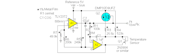
The circuit uses an integrator and a comparator. A FET switches between two values of collector current. A comparator drives the FET and also serves as the output. Rather than try to puzzle out the circuit just from the schematic, you can easily simulate it with LT Spice or Falstad. The Falstad simulator doesn’t have a way to change the temperature, but you can see it operating. The model isn’t good enough to really read a temperature, but you can see how the oscillation works
You can think of this as a temperature-to-frequency converter. It would be easy to read with, say, a microcontroller and convert the period to temperature. Every 10 microseconds is equal to a degree Kelvin. Not bad for something you don’t have to calibrate.
Thermistors are another way to measure temperature. Sometimes, you don’t need a sensor at all.