In the previous two HID articles, we talked about stealing HID descriptors, learned about a number of cool tools you can use for HID hacking on Linux, and created a touchscreen device. This time, let’s talk about an underappreciated HID standard, but one that you might be using right now as you’re reading this article – I2C-HID, or HID over I2C.
HID as a protocol can be tunneled over many different channels. If you’ve used a Bluetooth keyboard, for instance, you’ve used tunneled HID. For about ten years now, I2C-HID has been heavily present in laptop space, it was initially used in touchpads, later in touchscreens, and now also in sensor hubs. Yes, you can expose sensor data over HID, and if you have a clamshell (foldable) laptop, that’s how the rotation-determining accelerometer exposes its data to your OS.
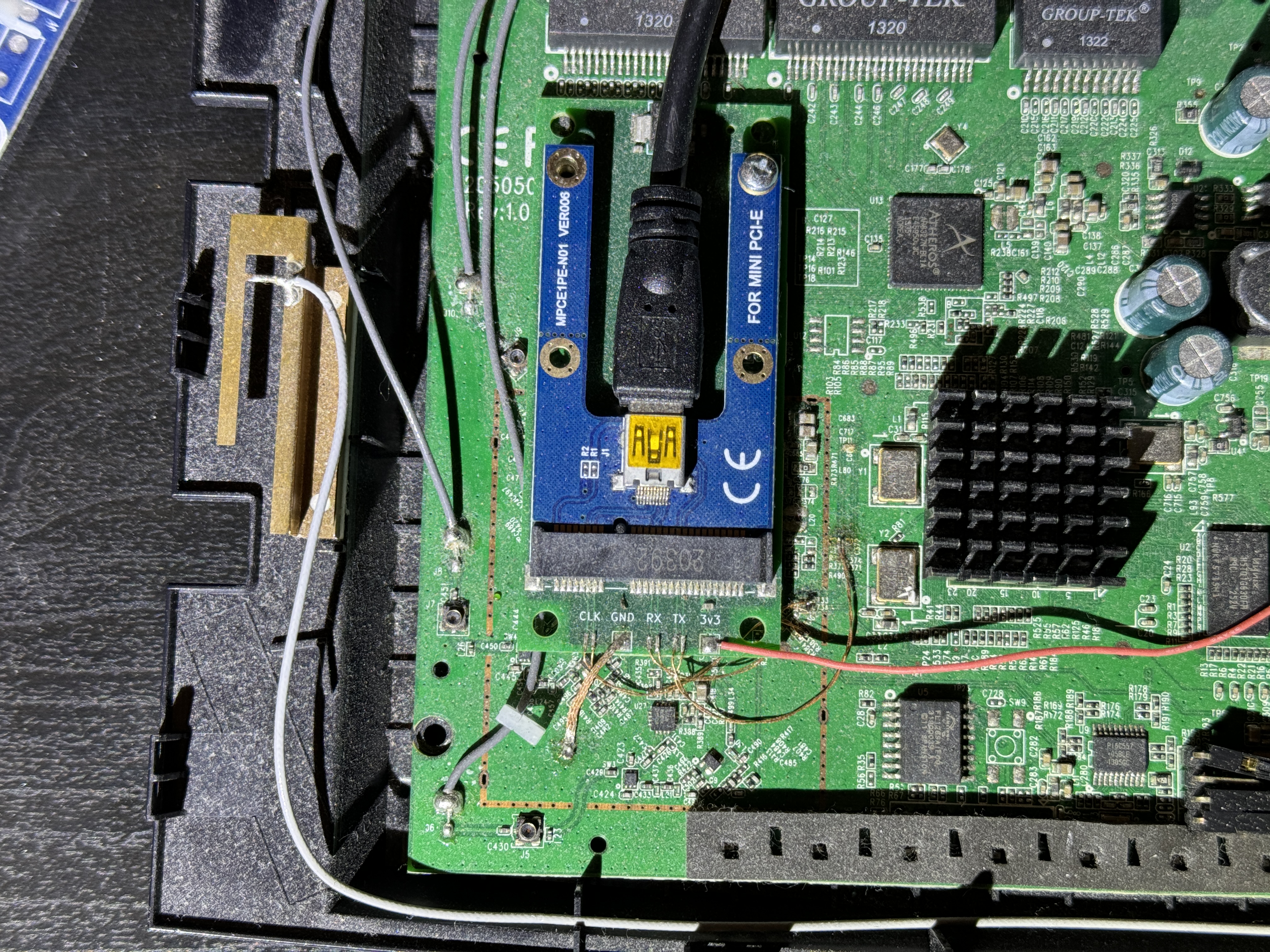
In modern world of input devices, I2C-HID is spreading, and the coolest thing is that it’s standardized. The standardization means a lot of great things for us hackers. For one, unlike all of those I2C touchscreen controllers, HID-I2C devices are easier to reuse; as much as information on them might be lacking at the moment, that’s what we’re combating right now as we speak! If you are using a recent laptop, the touchpad is most likely I2C-HID. Today, let’s take a look at converting one of those touchpads to USB HID.