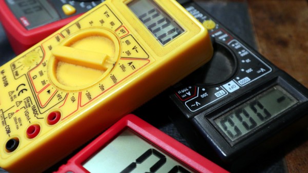
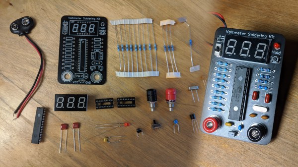
Grace Under Pressure: Shelley Green Celebrates Crimped Connections

We think it’s pretty safe to assume that most of the electrical connections our readers are making out there involve solder or solder paste. But we’ve all made a crimp connection or two in our lifetimes. Maybe you’ve squeezed a butt connector here and there, or made an Ethernet cable. Beyond getting the wiring order right in the Ethernet cable, how much did you wonder about what was happening inside the connector?

It may seem like solder is the superior option for making a low-resistance electrical connection. After all, you’re welding metals together with another metal. And this is usually all fine and good for circuit boards with sedentary indoor lives. But if a joint needs to be mechanically stable and survive in potentially harsh environments, you don’t want an alloy holding things together. You want metal to metal contact, and crimping is where it’s at.

A well-made crimp should last for several decades, but as Shelley Green explained in her talk at the 2019 Hackaday Superconference, good quality crimps don’t happen by accident. Good crimps are meticulously designed, and carefully executed from start to finish.

Continue reading “Grace Under Pressure: Shelley Green Celebrates Crimped Connections”

Defocused Laser Welding Fabric Proves There’s Many Ways To Slice It

Laser cutters are certainly a Hackerspace staple for cutting fabrics in some circles. But for the few fabrics derived from non-woven plastics, why not try fusing them together? That’s exactly what [Dries] did, and with some calibration, the result is a speedy means of seaming together two fabrics–no needles necessary!

The materials used here are non-woven goods often used in disposable PPE like face masks, disposable aprons, and shoe coverings. The common tool used to fuse non-woven fabrics at the seams is an ultrasonic welder. This is not as common in the hackerspace tool room, but laser cutters may be a suitable stand-in.

Getting the machine into a production mode of simply cranking out clothes took some work. Through numerous sample runs, [Dries] found that defocusing the laser to a spot size of 1.5mm at low power settings makes for a perfect threadless seam. The resulting test pockets are quite capable of taking a bit of hand abuse before tearing. Best of all, the fused fabrics can simply be cut out with another pass of the laser cutter. For fixtures, [Dries] started with small tests by stretching the two fabrics tightly over each other but suggests fixtures that can be pressed for larger patterns.

It’s great to see laser-cutters doubled-up as both the “glue” and “scissors” in a textile project. Once we get a handle on lasering our own set of scrubs, why not add some inflatables into the mix?

KiCad Panelization Made Easy

There’s a new Python-based script that will panelize your KiCad circuit boards from the command line. The project by [Jan Mrázek] is called KiKit and works on .kicad_pcb files to arrange them in a grid with your choice of mousebites or v-cuts for separating the boards after production.

When working with smaller boards it’s common practice to group them together into panels. This is done to speed up PCB assembly as multiple boards can have solder paste applied, go through a pick and place machine, and be sent into the reflow oven as a single unit. Often this is done manually, but in many cases this script will save you the time while delivering the results you need.

Let’s say you really wanted to make a whole bunch of those Xling open source Tamagotchi-like key fobs we saw a couple of weeks back. Using KiKit you can gang up six of the boards at a time, using “mousebites” to keep them together during production but make it easy to separate them after all the components are soldered:

/usr/local/bin/kikit panelize grid --space 3 --gridsize 2 3 --tabwidth 3 --tabheight 3 --htabs 2 --vtabs 1 --mousebites 0.5 1 0.25 --radius 1 Xling/hardware/xling.kicad_pcb xling_panel.kicad_pcb

You can see that the parameters let you set space between the boards, number of boards in the grid, width of the tabs, tab dimensions, number of tabs between boards, and even the radius of the curve where the tabs meet the board. These settings were pulled from the examples page, which demonstrates outcomes for many different settings options.

If you want to give this a try, we suggest installing directly from the repository, as improvements are ongoing and the pip3 version didn’t have all of the options shown in the examples. For us this was as easy as sudo python3 setup.py install and then calling the script with the full path /usr/local/bin/kikit.

Results from this board are both impressive and cautionary. You can see the top edge of the design is recessed yet the most up-to-date version of KiKit was still able to make the connection. However, how this affects the USB connector on the bottom of the board design may be something to consider before pulling the trigger on your panel order.

So. You Bought A VNA. Now What?

It’s never too late in life for new experiences, but there’s a new experience I had a few weeks ago that I wasn’t expecting. I probably received my first piece of test equipment – a multimeter –  in the early 1980s, and since then every time I’ve received a new one, whether an oscilloscope, logic analyser, spectrum analyser or signal generator, I’ve been able to figure out how to use it. I have a good idea what it does, and I can figure out whatever its interface may be to make it do what I want it to. My new experience came when I bought a piece of test equipment, and for the first time in my life didn’t have a clue how to use it.

That instrument is a Vector Network Analyser, or VNA, and it’s worth spending a while going through the basics in case anyone else is in the same position. My VNA is not a superlative piece of high-end instrumentation that cost the GDP of a small country, it’s the popular $50 NanoVNA that has a fairly modest frequency range and performance, but is still a functional VNA that can take useful measurements. But I’m a VNA newbie, what does a VNA do? Continue reading “So. You Bought A VNA. Now What?”

Printed It: Collet Drill Stop

You’d think that being quarantined in your home would be perfect for hackers and makers like us, as we all have a project or two that’s been sitting on the back burner because we didn’t have the time to tackle it. Unfortunately, some are finding that the problem now is actually getting the parts and tools needed to do the job. When there’s a bouncer and a line outside the Home Depot like it’s a nightclub on Saturday night, even the simplest of things can be difficult to source when making in the time of COVID.

Which is exactly the situation I found myself in recently when I needed to drill a bunch of holes to the same depth. The piece was too big to put in the drill press, and while I contemplated just wrapping the bit in some tape to serve as a makeshift stop, I wasn’t convinced it would be accurate or repeatable enough. It occurred to me that a set of drill stop collars would be easy enough to design and 3D print, but before I fired up OpenSCAD, I decided to see what was already available online.

Which is how I found the “Collet Drill Stop” from Adam Harrison. Rather than the traditional ring and setscrew arrangement, his design uses a printable collet that will clamp down on the bit at an arbitrary position without tools. So not only could I avoid a trip to the store by printing this design out, it looked like it would potentially be an upgrade over what I would have bought.

Of course, it’s wise not to take anything for granted when dealing with 3D printing. The only way I could be sure that Adam’s design would work for me was to commit it to plastic and try it out.

Continue reading “Printed It: Collet Drill Stop”

Have JBC Soldering Handle, Will USB-C Power Deliver

Frequent converter-of-tools-to-USB-C [Jana Marie Hemsing] is at it again, this time with a board to facilitate using USB Power Delivery to fuel JBC soldering iron handles. Last time we saw [Jana] work her USB-C magic was with the Otter-Iron, which brought Power Delivery to the trusty TS100 with a purpose built replacement PCBA. This time he’s taking a different approach by replacing the “station” of a conventional soldering station completely with one tiny board and one giant capacitor.

If you’ve been exposed to the “AC fire starter” grade of soldering iron the name JBC might be unfamiliar. They make tools most commonly found with Metcal’s and high end HAKKOs and Wellers on the benches of rework technicians and factory floors. Like any tool in this class each soldering station comes apart and each constituent piece (tips, handles, base stations, stands, etc) are available separately from the manufacturer and on the used market at often reasonable prices, which is where [Jana] comes in.

The Otter-Iron PRO is a diminutive PCBA which accepts a USB-C cable on one side and the connector from a standard JBC T245-A handle on the other. JBC uses a fairly typical thermistor embedded in the very end of the iron tip, which the Otter-Iron PRO senses to provide closed loop temperature control. [Jana] says it can reach its temperature setpoint from a cold start in 5 seconds, which roughly matches the performance of an original JBC base station! We’re especially excited because this doesn’t require any modification to the handle or station itself, making it a great option for JBC users with a need for mobility.

Want to make an Otter-Iron PRO of your own? Sources are at the link at the top. It sounds like v3 of the design is coming soon, which will include its own elegant PCB case. Check out the CAD render after the break. Still wondering how all this USB-PD stuff works? Check out [Jason Cerudolo’s] excellent walkthrough we wrote up last year.

Continue reading “Have JBC Soldering Handle, Will USB-C Power Deliver”

Tubes Have Character With A Tek 570

When tubes were king, you could go to a drugstore with a box full of them from your TV. There would be a tester that would tell you what tubes were bad and, of course, you could buy the replacements for them. That kind of tube tester was pretty simple. If you wanted to really know how to design with a tube or test its parameters, you were much better off with a curve tracer like the Tektronix 570 that [tomtektest] shows off in two recent videos that you can see below.

That piece of kit fell into [Tom’s] lap thanks to an observant delivery driver. The 1955 instrument is very similar to a semiconductor curve tracer but, of course, has the ability to provide much higher voltage for the tubes. The basic idea is that the X axis sweeps from a few volts up to 100s of volts. The vertical scale will show the plate, screen, or grid current. From those curves you can learn a lot about the characteristics of the tube.

Continue reading “Tubes Have Character With A Tek 570”