Benchmarking Chinese CPUs

When it comes to PCs, Westerners are most most familiar with x86/x64 processors from Intel and AMD, with Apple Silicon taking up a significant market share, too. However, in China, a relatively new CPU architecture is on the rise. A fabless semiconductor company called Loongson has been producing chips with its LoongArch architecture since 2021. These chips remain rare outside China, but some in the West have been benchmarking them.

[Daniel Lemire] has recently blogged about the performance of the Loongson 3A6000, which debuted in late 2023. The chip was put through a range of simple benchmarking tests, involving float processing and string transcoding operations. [Daniel] compared it to the Intel Xeon Gold 6338 from 2021, noting the Intel chip pretty much performed better across the board. No surprise given its extra clock rate. Meanwhile, the gang over at [Chips and Cheese] ran even more exhaustive tests on the same chip last year. The Loongson was put through typical tasks like  compressing archives and encoding video. The outlet came to the conclusion that the chip was a little weaker than older CPUs like AMD’s Zen 2 line and Intel’s 10th generation Core chips. It’s also limited as a four-core chip compared to modern Intel and AMD lines that often start at 6 cores as a minimum.

If you find yourself interested in Loongson’s product, don’t get too excited. They’re not exactly easy to lay your hands on outside of China, and even the company’s own website is difficult to access from beyond those shores. You might try reaching out to Loongson-oriented online communities if you seek such hardware.

Different CPU architectures have perhaps never been more relevant, particularly as we see the x86 stalwarts doing battle with the rise of desktop and laptop ARM processors. If you’ve found something interesting regarding another obscure kind of CPU, don’t hesitate to let the tipsline know!

Musings On A Good Parallel Computer

Until the late 1990s, the concept of a 3D accelerator card was something generally associated with high-end workstations. Video games and kin would run happily on the CPU in one’s desktop system, with later extensions like MMX, 3DNow!, and SSE providing a significant performance boost for games that supported them. As 3D accelerator cards (colloquially called graphics processing units, or GPUs) became prevalent, they took over almost all SIMD vector tasks, but one thing that they’re not good at is being a general-purpose parallel computer. This really ticked [Raph Levien] off and it inspired him to cover his grievances.

Although the interaction between CPUs and GPUs has become tighter over the decades, with PCIe in particular being a big improvement over AGP and PCI, GPUs are still terrible at running arbitrary computing tasks, and even PCIe links are still glacial compared to communication within the GPU and CPU dies. With the introduction of asynchronous graphic APIs this divide became even more intense. [Raph]’s proposal is to invert this relationship.

There’s precedent for this already, with Intel’s Larrabee and IBM’s Cell processor merging CPU and GPU characteristics on a single die, though both struggled with developing for such a new kind of architecture. Sony’s PlayStation 3 was forced to add a GPU due to these issues. There is also the DirectStorage API in DirectX, which bypasses the CPU when loading assets from storage, effectively adding CPU features to GPUs.

As [Raph] notes, so-called AI accelerators also have these characteristics, with often multiple SIMD-capable, CPU-like cores. Maybe the future is Cell after all.

Close-up of a CPU

Register Renaming: The Art Of Parallel Processing

In the quest for faster computing, modern CPUs have turned to innovative techniques to optimize instruction execution. One such technique, register renaming, is a crucial component that helps us achieve the impressive multi-tasking abilities of modern processors. If you’re keen on hacking or tinkering with how CPUs manage tasks, this is one concept you’ll want to understand. Here’s a breakdown of how it works and you can watch the video, below.

In a nutshell, register renaming allows CPUs to bypass the restrictions imposed by a limited number of registers. Consider a scenario where two operations need to access the same register at once: without renaming, the CPU would be stuck, having to wait for one task to complete before starting another. Enter the renaming trick—registers are reassigned on the fly, so different tasks can use the same logical register but physically reside in different slots. This drastically reduces idle time and boosts parallel tasking. Of course, you also have to ensure that the register you are using has the correct contents at the time you are using it, but there are many ways to solve that problem. The basic technique dates back to some IBM System/360 computers and other high-performance mainframes.

Register renaming isn’t the only way to solve this problem. There’s a lot that goes into a superscalar CPU.

Continue reading “Register Renaming: The Art Of Parallel Processing”

What Happens If You Speedrun Making A CPU?

Usually, designing a CPU is a lengthy process, especially so if you’re making a new ISA too. This is something that can take months or even years before you first get code to run. But what if it wasn’t? What if one were to try to make a CPU as fast as humanly possible? That’s what I asked myself a couple weeks ago.

Left-to-right: Green, orange and red rectangle with 1:2 aspect ratio. Each rectangle further right has 4x the area of its neighbor on the left.
Relative ROM size. Left: Stovepipe, center: [Ben Eater]’s, right: GR8CPU Rev. 2
Enter the “Stovepipe” CPU (I don’t have an explanation for that name other than that I “needed” one). Stovepipe’s hardware was made in under 4 hours, excluding a couple small bugfixes. I started by designing the ISA, which is the simplest ISA I ever made. Instead of continuously adding things to make it more useful, I removed things that weren’t strictly necessary until I was satisfied. Eventually, all that was left were 8 major opcodes and a mere 512 bits to represent it all. That is far less than GR8CPU (8192 bit), my previous in this class of CPU, and still less than [Ben Eater]’s breadboard CPU (2048 bit), which is actually less flexible than Stovepipe. All that while taking orders of magnitude less time to create than either larger CPU. How does that compare to other CPUs? And: How is that possible?
Continue reading “What Happens If You Speedrun Making A CPU?”

Why X86 Needs To Die

As I’m sure many of you know, x86 architecture has been around for quite some time. It has its roots in Intel’s early 8086 processor, the first in the family. Indeed, even the original 8086 inherits a small amount of architectural structure from Intel’s 8-bit predecessors, dating all the way back to the 8008. But the 8086 evolved into the 186, 286, 386, 486, and then they got names: Pentium would have been the 586.

Along the way, new instructions were added, but the core of the x86 instruction set was retained. And a lot of effort was spent making the same instructions faster and faster. This has become so extreme that, even though the 8086 and modern Xeon processors can both run a common subset of code, the two CPUs architecturally look about as far apart as they possibly could.

So here we are today, with even the highest-end x86 CPUs still supporting the archaic 8086 real mode, where the CPU can address memory directly, without any redirection. Having this level of backwards compatibility can cause problems, especially with respect to multitasking and memory protection, but it was a feature of previous chips, so it’s a feature of current x86 designs. And there’s more!

I think it’s time to put a lot of the legacy of the 8086 to rest, and let the modern processors run free. Continue reading “Why X86 Needs To Die”

Minecraft In Minecraft On The CHUNGUS II

Minecraft is a simple video game. Well, it’s a simple video game that also has within it the ability to create all of the logic components that you’d need to build a computer. And building CPUs in Minecraft is by now a long-standing tradition.

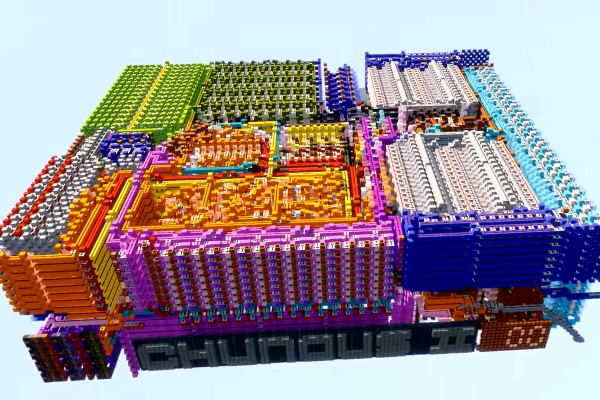
Enter CHUNGUS II. The Computational Humongous Unconventional Number and Graphics Unit by [Sammyuri] is the biggest and baddest Minecraft computer that we’ve ever seen. So big, in fact, that it was finally reasonable to think about porting a stripped-down version of Minecraft to the computer itself. Yes, that’s right, Minecraft running in Minecraft. (Video embedded below.) Writing the compiler and programming the game brought two more hackers to the party, [Uwerta] and [StackDoubleFlow], and quite honestly, we’re amazed that a team as small as three people pulled this off.

Anyway, once you’ve picked your jaw up off the floor, also check out [Sammyuri]’s video on just the CHUNGUS II computer itself. (Also embedded below.) Seeing the architecture is interesting, even if you don’t speak Redstone as fluently as our heroes here. We love that the assembler creates a block of ROM – out of Minecraft blocks – that you can then cut/paste into the game’s reality.

For a “simple” game about breaking blocks and punching trees, Minecraft has inspired hackers to make the game better both inside and outside of the real world. For instance, for the latest in performant open-source Minecraft servers, check out Folia. Maybe, one day, they’ll build CHUNGUS II in the real world. It could happen.

Thanks [dbcdr] for the tip!

Continue reading “Minecraft In Minecraft On The CHUNGUS II”

History Of The SPARC CPU Architecture

[RetroBytes] nicely presents the curious history of the SPARC processor architecture. SPARC, short for Scalable Processor Architecture, defined some of the most commercially successful RISC processors during the 1980s and 1990s. SPARC was initially developed by Sun Microsystems, which most of us associate the SPARC but while most computer architectures are controlled by a single company, SPARC was championed by dozens of players.  The history of SPARC is not simply the history of Sun.

A Reduced Instruction Set Computer (RISC) design is based on an Instruction Set Architecture (ISA) that runs a limited number of simpler instructions than a Complex Instruction Set Computer (CISC) based on an ISA that comprises more, and more complex, instructions. With RISC leveraging simpler instructions, it generally requires a longer sequence of those simple instructions to complete the same task as fewer complex instructions in a CISC computer. The trade-off being the simple (more efficient) RISC instructions are usually run faster (at a higher clock rate) and in a highly pipelined fashion. Our overview of the modern ISA battles presents how the days of CISC are essentially over. Continue reading “History Of The SPARC CPU Architecture”