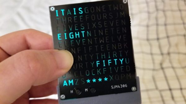
Everyone seems to love word clocks. Maybe it’s the mystery of a blank surface lighting up to piece together the time in fuzzy format, or maybe it hearkens back to those “find-a-word” puzzles that idled away many an hour. Whatever it is, we see a lot of word clock builds, but there’s something especially about this diminutive PCB word clock that we find irresistible.
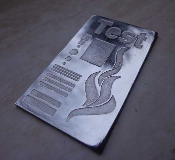
Like all fun projects, [sjm4306] found himself going through quite the design process with this one. The basic idea – using a PCB as the mask for the character array – is pretty clever. We’ve always found the laser-cut masks to be wanting, particularly in the characters with so-called counters, those enclosed spaces such as those in a capital A or Q that would be removed by a laser cutter. The character mask PCB [sjm4306] designed uses both the copper and a black solder mask to form the letters, which when lit by the array of SMD LEDs behind it glow a pleasing blue-green color against a dark background. Try as he might, though, the light from adjacent cells bled through, so he printed a stand that incorporates baffles for each LED. The clock looks great and even has some value-added modes, such as a falling characters display a la The Matrix, a Pong-like mode, and something that looks a bit like Tetris. Check out the video below for more details.
We’ve seen word clocks run afoul of the counter problem before, some that solved it by resorting to a stencil font, others that didn’t. We’re impressed by this solution, though, enough so that we hope [sjm4306] makes the PCB files available so we can build one.
Continue reading “LEDs Shine Through PCB On This Tiny Word Clock”
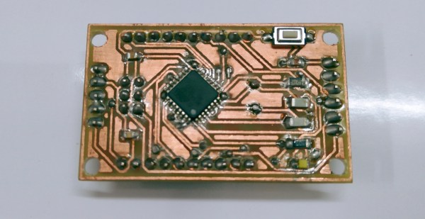
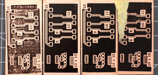
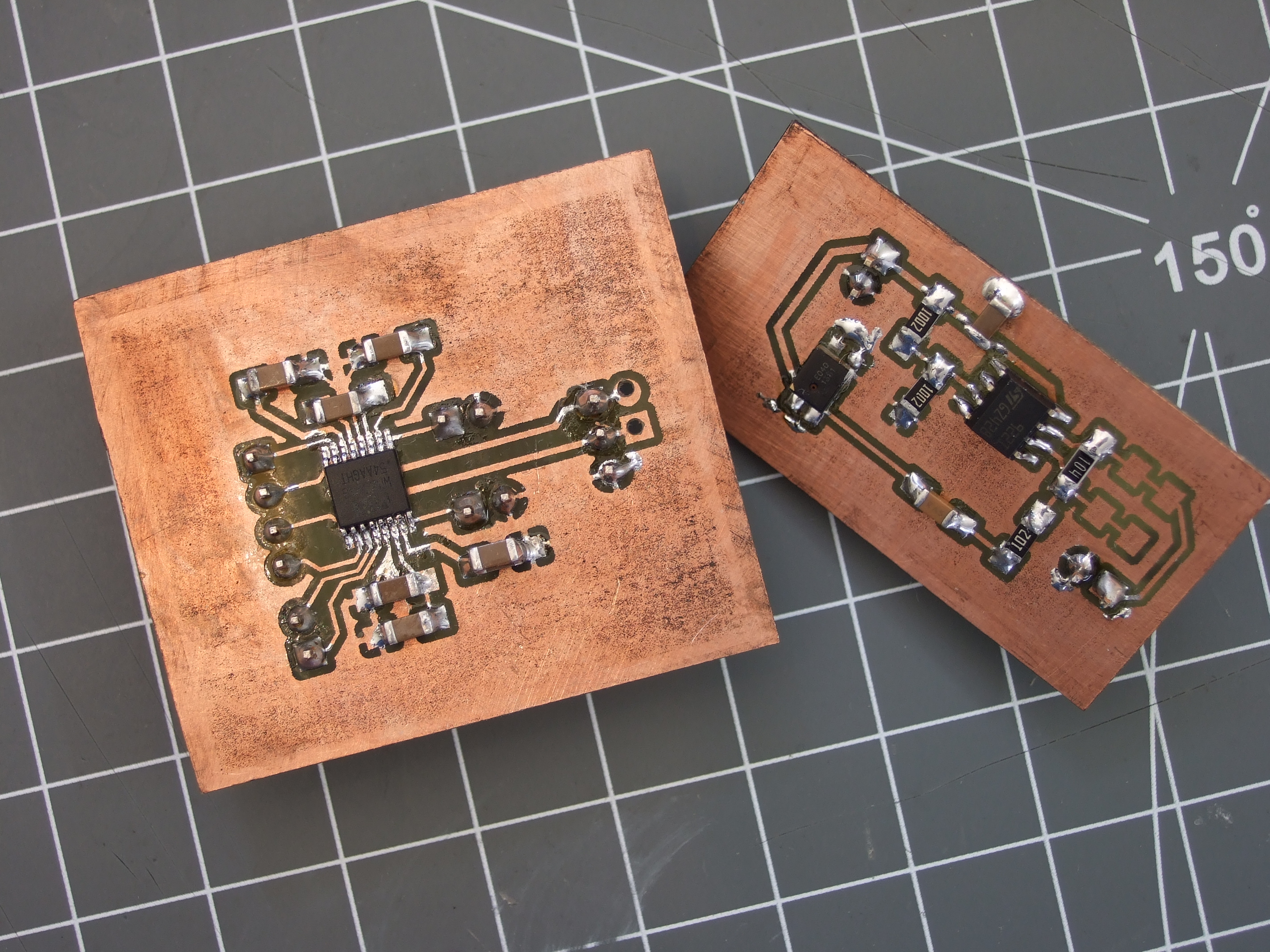
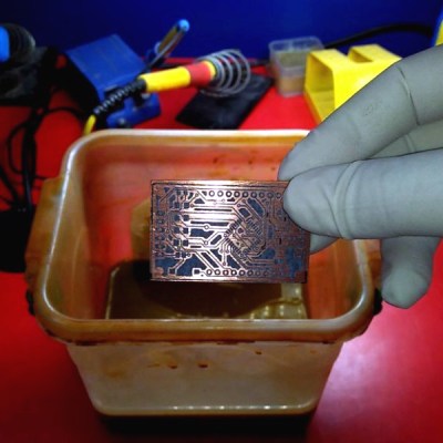 [Pratik Makwana] starts by showing how to design the circuit schematic diagram in an EDA tool (Eagle) and the corresponding PCB layout design. He then uses the toner transfer method and a laminator to imprint the circuit into the copper board for later etching and drilling. The challenging soldering process is not detailed, if you need some help soldering SMD sized components we covered some different processes before, from a