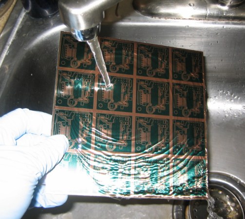
We think that anyone who’s done at-home PCB fabrication will appreciate the tidiness that [Fran] maintains throughout her etching process. She recently posted a three-part video tutorial which showcases her techniques. As you can see in the screenshot above, her habits reek of top-notch laboratory skills.
Regular readers can probably guess what circuit she’s etching. It’s the test boards for her LVDC reverse engineering. She is using the toner transfer method, but in a bit different way than most home-etchers do. She uses the blue transfer paper made for the job, but before transferring it to the copper clad she uses a light box (kind of like the X-ray film viewer at the doctor’s office) to inspect for any gaps where toner did not adhere. From there she uses a heat press to apply the resist. This is a heck of a lot easier than using a clothes iron, but of course you’ve got to have one of these things on hand to do it this way.
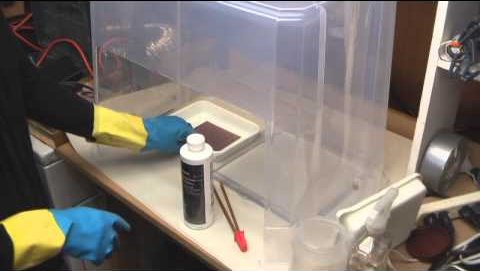
The second part of the tutorial is embedded after the break. We chose this segment because it shows off how [Fran] built her own chemical hood. It’s a clear plastic storage container lying upside down. A work window has been cut out of the front side, and a 4-inch exhaust hose added to the top. [Fran’s] lab has a high volume low velocity fan to which it connects to whisk the fumes outside.