[Clifford] presented a fully open-source toolchain for programming FPGAs. If you don’t think that this is an impressive piece of work, you don’t really understand FPGAs.
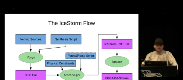
The toolchain, or “flow” as the FPGA kids like to call it, consists of three parts: Project IceStorm, a low-level tool that can build the bitstreams that flip individual bits inside the FPGA, Arachne-pnr, a place-and-route tool that turns a symbolic netlist into the physical stuff that IceStorm needs, and Yosys which synthesizes Verilog code into the netlists needed by Arachne. [Clifford] developed both IceStorm and Yosys, so he knows what he’s talking about.
What’s most impressive is that FPGAs aren’t the only target for this flow. Because it’s all open source and modifiable, it has also been used for designing custom ASICs, good to know when you’re in need of your own custom silicon. [Clifford]’s main focus in Yosys is on formal verification — making sure that the FPGA will behave as intended in the Verilog code. A fully open-source toolchain makes working on this task possible.
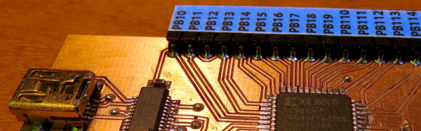
If you’ve been following along with [Al Williams]’s FPGA posts, either this introduction or his more recent intermediate series that are also based on the relatively cheap Lattice iCEStick development kit, this video is a must-watch. It’s a fantastic introduction to the cutting-edge in free FPGA tools.