Put A Solder Mask On Those Homebrew PCBs

While making your own PCBs at home is one of the best marks of a competent builder, if you want to give your project a more professional vibe, you’re going to need to do better than bare copper traces on a piece of fiberglass. To help out his fellow makers, [Chris] sent in his Instructable on creating a solder mask for homemade circuit boards using a minimal amount of tools and materials easily sourced from the Internet.

[Chris]’ soldermasks are made from UV curing paints he found on eBay. Of course the traditional green paint is available, along with paints very similar to the Sparkfun red or Arduino blue soldermasks.

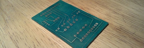
After brushing the soldermask paint onto his home-etched circuit board, [Chris] printed out the solder mask onto a piece of transparency film using a laser printer. This mask is vitally important if you ever plan to solder your board; by covering the pads you wish to solder, the paint won’t cure and can later be removed.

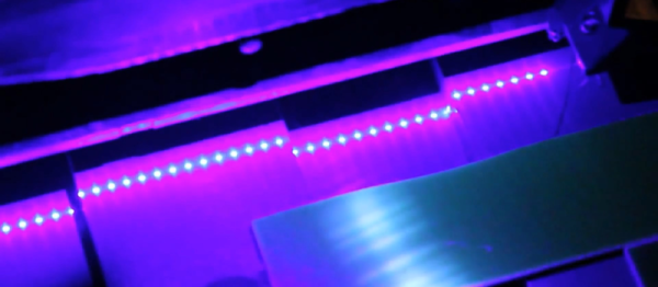
[Chris] cured his soldermask by leaving it in the sun for a half hour. After the paint was dry, he removed the excess paint covering the pads with a little bit of turpentine and some elbow grease.

While [Chris]’ paint had somewhat of an ugly matte finish, the soldermask does its job, protecting the PCB traces while leaving the pads uncovered and ready to solder.

Etching Your Own PCBs At Home

Etching your own PCBs from copper clad board is nothing new, but the ability to make your own circuit boards at home is so useful it should be part of every maker’s repertoire of skills. The folks over at Hub City Labs in Moncton, NB, Canada put together a workshop covering the basics of home PCB manufacturing, allowing any maker to put a circuit board in their hands in under an hour.

The process starts just like any PCB design – laying out traces, parts, and vias in a PCB designer such as Eagle. When making your own boards, it’s a good idea to make the traces and pads extra large; the folks at Hub City Labs follow the 50-50 rule: 50 mil wide traces with 50 mils of seperation.

The PCB design is printed out with a laser printer (in mirror mode) onto a piece of paper from a glossy magazine or inkjet photo paper. After the copper board is scrubbed to remove any oxidation or oils present, the design is laid face down on the copper and heated with a clothes iron or sent through a laminator.

After the laser printer toner is transferred to the copper, the recipe calls for etching the board with a solution consisting of a half cup of 3% Hydrogen Peroxide and a quarter cup of muriatic acid.

The folks at Hub City Labs put together a great tutorial for one of the most useful skills the home electronics wizard can have, but etching your own PCBs is an art unto itself. There’s a lot of ways this process can be improved, from using Kapton tape to secure the printed art to the copper board, to getting high-strength peroxide from a beauty supply store.

If you’ve got any tips on making your own PCBs at home, drop a line in the comments below.

EDIT: Good job killing Hub City Lab’s web server, everybody. They’re working on getting something up.

BGA Soldering With A Paint Stripper And Stopwatch

Having just received a shiny set of PCBs from the fab-house [Devbisme] needed a way to solder the main chip in place. It has a Ball-Grid Array footprint which is notoriously difficult to populate in a home lab. But he makes it look pretty easy and decided to share a video tutorial of the process.

The main tool he used is the paint stripper (heat gun) seen above. Since he didn’t have his own fancy reflow oven he made things work with the gun as his heat source. First he applies a generous layer of liquid solder flux to the BGA footprint on the board. Next he melts some solder onto the tip of his iron and uses it to tin all of the board’s BGA pads. Then it’s time for the critical step of positioning the chip. He uses vacuum tweezers to set it in place, and traditional tweezers to fine-tune its position. From here he heats with the paint stripper for two minutes, starting far above the board and slowly moving closer, with the reverse at the end of the soldering process. Once cool the board is cleaned with distilled water and blown dry with compressed air. After a visual inspection he finishes the application with a 30 minute stay in a 300 degree oven. We’ve included the video after the break for your convenience.

We’ve seen a similar technique used for replacing a chip on an already populated board.

Continue reading “BGA Soldering With A Paint Stripper And Stopwatch”

Toorcamp: Milling PCBs With KiCad

[Hao] from Noisebridge showed me their CNC mill being used to etch PCBs. Using copper clad board, this MAXNC 10 mill routes the PCB with decent accuracy. This makes for very rapid prototyping of single sided PCBs.

[Hao] designed the PCB using the open source KiCad EDA tool. This was used to draw the schematic, layout the PCB, and generate the Gerber files. Next, pcb2gcode was used to convert the Gerbers to G-code, which is a standard set of instructions for controlling CNC devices. Finally, LinuxCNC was used to send the G-code instructions to the mill. It’s a powerful application of a completely open source workflow.

The PCB being milled is for a pressure based touch sensor. It uses the Freescale MPL115A barometric pressure sensor encased in a rubber housing. This sensor is being incorporated into the Dora Opensource Robot Assistant project, which [Hao] and the Noisebridge folks are working on. We’re looking forward to hearing more about the Dora project in the future.

Birth Of An Arduino

Hey look, an Arduino without its clothes on. This one’s just started its journey to becoming the ubiquitous prototyping tool. The image is from [Bunnie’s] recent tour of the fab house where Arduino boards are made.

As it says on every true Arduino board, they’re made in Italy. [Bunnie’s] trip to the factory happened in Scarmagno, on the outskirts of Torino. The process starts with large sheets of FR4 copper clad material, usually about 1 by 1.5 meters in size. The first task is to send the sheets through a CNC drill. With all of the holes done it’s time for some etch resist; the image above is just after the resist has been applied. A robotic system takes over from here, running the panels through the chemicals which first etch away the copper, then remove the resist and plate the remaining traces. From there it’s off to another machine for solder mask and silk screen.

There are videos of each step available. But our favorite piece is the image at the end that shows a pallet with stacks of completed PCB panels which are headed off to be populated with components.

[via Reddit]

Exposing PCBs With A Home Made Laser Printer

Making your own printed circuit boards – as useful as it is – is a pain. Using the very popular toner transfer method requires a dozen steps that have to go perfectly the first time, and milling boards on a CNC machine creates a lot of mess. The most industrious hackers are able to bodge up a direct-to-board printer from an old inkjet printer, but these builds are usually a little kludgy. [Tixiv]’s LaserExposer board printer is one of the first builds we’ve seen that does away with all the negatives of the other techniques of PCB manufacturing and turns making your own boards into a very, very simple process.

The LaserExposer uses photosensitive copper board, like many of the other PCB printers we’ve seen. Instead of printing out the board artwork to a transparency or mask, [Tixiv] used a 1 Watt 445nm blue laser with a hexagonal mirror to directly expose the artwork onto the board, line by line.

The entire device is built around an old flatbed scanner that slowly crawls over the PCB, exposing the traces of copper to be etched away. This required reverse engineering the mirror motor control board from an 90s-era laser printer and building a circuit to precisely control the timing of the laser. [Tixiv] eventually got everything working and after etching had some of the most professional looking home-brew boards we’ve ever seen.

[Tixiv] put up a demo video of his build (after the break, German audio, YouTube has captions…). Anyone have an old flatbed scanner lying around?

Continue reading “Exposing PCBs With A Home Made Laser Printer”

Designing A Quadcopter Brain PCB

When working on his quadcopter project [Matt] decided it would be best to build a robust controller for the device. He had never sent off a PCB design for fabrication, but took the plunge and ended up with a compact and reliable PCB on the first try.

One of the first things that comes to mind when we hear about quadcopter controllers are the feedback sensors. The accelerometers which are used for these projects generally come in a DFN or QFN package. This means there are no legs. Instead the chip has pads on the bottom of the package making it a lot more difficult to solder. [Matt] side-stepped this issue by using an IMU board which already has the sensors in place and offered a 0.1″ SIL pin header to use as an interface. This is simple to roll into the design, along with all of the other connectors for motor control, power, etc. He grabbed a copy of Eagle Lite to do the layout, and used OSH Park to get the boards fabricated. He was surprised that everything worked on the first try. Thanks to his planning it fits inside of a plastic food container where it should be able to ride out most minor crashes with ease.