Bitten By PCB Defects

If you’ve ordered PCBs from Seeed Studio, ITead, DirtyPCB, or another board house in China, you’ve probably noticed that neat little 100% e-test option available on the order form. If you select this, the board house will throw your PCBs in a machine that will poke a pin in every pad to make sure all the connections are good. Less work for you, right? As [Andy] found out, not always. He was bitten by a manufacturing defect that sheds some light on what that e-test actually is, and the capabilities of what these Chinese board houses can do.

Most of [Andy]’s project have a lot of surface mount components, and when he receives his boards, he notices a few pin pricks on each and every pad. This is from a flying lead machine; a robotic continuity checker that makes sure all the relevant pads are electrically isolated from each other.

One of [Andy]’s recent projects is an entirely through-hole design. Apparently these robotic meters don’t test through-hole pads; it’s significantly harder to measure the continuity of a hole rather than a pad, apparently. After assembling one of these boards, he noticed a problem where one of the GPIOs was permanently high. The offending trace was found underneath a DIP socket, in precisely the worst possible place it could be.

If [Andy] had inspected the board beforehand, this problem would have been avoided. He says it was a relatively simple board with big traces and wide spaces and he didn’t think a manufacturing defect was possible. He was wrong, and now we have a warning. We thank him for that.

The Ultimate Tool For Homebrew PCB Manufacturing

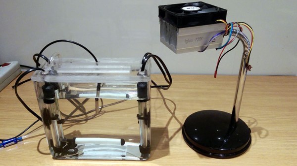
While OSHPark, Seeed Studio, and DirtyPCB have taken most of the fun and urgency out of making your own circuit boards at home, there are still a few niche cases and weird people who like to go it alone. For them, [Jarzębski] has created the ultimate homebrew PCB manufacturing solution (.pl, here’s the Google translatrix).

[Jarzębski] is using UV-sensitive photomasks for his PCBs, but he’s not doing something simple like a blacklight to develop his boards. He’s using a 30 Watt UV LED for exposing his boards. This, of course, generates a lot of heat and to mitigate that he’s added a Peltier cooler, temperature sensor, and a fan to cool off this retina-burning LED. 30 Watts will get the job done, considering [Jarzębski] was using a quartet of 4.5W LEDs before this build.

Developing a PCB is only one part of the equation; you need to etch it, too. For this, [Jarzębski] is using a small 1.6 Liter aquarium and four aquarium heaters for dunking 120mm x 120mm PCBs in the tank. There’s no mention of what chemistry [Jarzębski] is using – ferric chloride, cupric chloride, or otherwise – but the heaters and aerator should make etching go very smoothly.

There’s a video (English) going over the rest of the project below.

Continue reading “The Ultimate Tool For Homebrew PCB Manufacturing”

DIY Mini-Drill Would Make Mad Max Proud

mini-drill

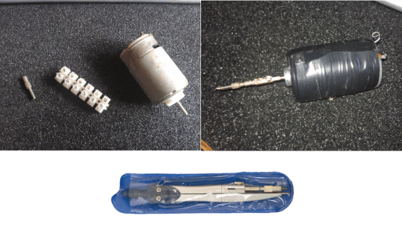
That’s not a prison tattoo gun up there, it’s [Szabolcs] DIY mini drill. Hackaday has been on a bit of a DIY tool kick lately – with improvised saws, grinders, and grinders converted to saws, among other things. We haven’t had any DIY drills yet, though. [Szabolcs] needed a drill for his home-made printed circuit boards. Usually a Dremel or similar rotary tool is pressed into service for drilling PCBs. However, for some reason he didn’t have access to one. [Szabolcs] called upon his inner MacGyver and built a drill from parts he had on hand.

Every drill needs a chuck, or at least a collet holder. This drill’s chuck is sourced from a drafting compass. Long ago in the dark ages before CAD, mechanical drawings were manually drawn up. Companies employed entire drafting departments to draw designs, blueprints, and schematics. These draftsmen used the compass to create accurate circles and arcs. [Szabolcs] re-used the lead holder from the compass as a chuck for his drill. A 540 or 550 brushed sealed endbell can motor, common to the R/C cars spins the drill up. We originally thought [Szabolcs] used an Erector or Meccano set piece as a shaft coupling. The truth is it’s the internals of a Euro style terminal strip. A small tactile button is used to activate the motor. Some electrical tape wrapped around the motor holds the button in place. The tape also makes sure that the user isn’t cut by the sheet metal field ring wrapped around the can. Power for the system can come from just about anywhere, though [Szabolcs] says he uses the 12v rail of an old ATX power supply.

3D Printed, Solderless Circuits

3d printed board

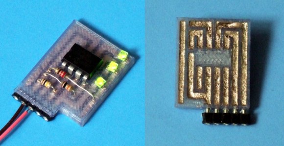
If you’re looking for yet another alternative to etching your own PCBs, then check out this new Instructable on 3D printing test circuits!

[Mikey] decided to try out this method when he needed a small board prototype. He designed the perfboard to have a standard thickness—only 1/16th thick (~1.6mm)—with thin, recessed channels on one side and through holes on the other. [Mikey’s] circuit board allows you to stuff your components in, hold them down with a piece of tape, and then fill the channels with some kind of conductive material. In this example he’s used a highly conductive paint.

This 3D printed option probably won’t suit all your circuit-building needs, but it could provide an excellent shortcut for your next hack! As always, there’s a video after the break.

Continue reading “3D Printed, Solderless Circuits”

Recreate A PCB With A Scanner And Inkscape

turnsig

[John] has managed to replace a broken turn signal PCB by scanning it and converting to Gerber format. [John] purchased a Triumph Spitfire with toggle switch wired up for turn signal control. The “official” replacement part worked better than the toggle switch, but it didn’t cancel after turning. He was able to get the original switch, only to find it had a hole completely burned through the phenolic board. This isn’t completely surprising, as Triumph used a Lucas Industries electrical system. As anyone who has owned a car with a Lucas “prince of darkness” electrical system will tell you, Lucas systems were not known for quality. A quick Google search brings up plenty of pages attesting to this.

Phenolic resin/paper was a common early PCB material.  The FR-4 fiberglass boards most commonly used today could be considered descendants of FR-1 and FR-2 phenolic. (The FR in this case stands for Fiber Reinforced). The standardization worked in [John’s] favor, as his burned board was 31 mils thick, which is still a standard PCB thickness. Re-creating an odd sized board such as this isn’t a hard job. It would however mean spending quite a bit of time with a ruler and a caliper. Rather than spend all that time measuring and re-drawing, [John] scanned his PCB on a flatbed scanner. He used graph paper as a background to verify the image wasn’t being stretched or skewed.

[John] brought his scan into inkscape, and traced both the outline and copper areas. The outline and copper had to be exported as two separate files, so he added corner marks outside the board outline as fiducials.  He then used pstoedit to convert inkscape’s eps output files to gEDA pcb format. The two files were rejoined in gEDA. From there [John] exported a Gerber, and ran it on his home PCB milling machine.  The results look good. [John] plans to make another revision of the board from a professional PCB house with vias to hold the copper to the substrate.

CNC Software Toolchain Using Only Open Source Software

For hobbyists, there are two types of machines that can make parts at home. The first type is matter-adding machines (3D printers) and the other is matter-subtracting machines (like CNC milling machines).  [Mario] recently tipped us about an article he made detailing which free software can be used to design and produce parts on CNC machines.

The first step of the process is obviously designing the part you want to make using a Computer-Aided Design (CAD) application. [Mario] suggests Heeks or Freecad for which you can find plenty of tutorials on YouTube. The next step consists in converting the part you just designed to machine tool paths using a Computer-Aided Manufacturing (CAM) application. Fortunately, Heeks can do both so it may be the best option for beginners. [Mario] also mentions the pcb2gcode  application, which allows you to manufacture printed circuit boards at home for the prototypes you may want to produce. Finally, the well known LinuxCNC (previously Linux EMC2) software is used to control the CNC machine using the GCode that the CAM software produced.

At Hackaday, we’d really like knowing what our readers currently use for their CNCs so don’t hesitate to leave us a comment below.

DIY Heatsinking PCBs

pcb heatsink

We have covered many do it yourself PCBs before, but this video guide adds an easy way to sink heat from high power devices, which we think you might find handy.

It is a very simple process that [CNLohr] uses to keep his small RGB LED projects from overheating. It starts by using a readily available silicone thermal sheet as the substrate by applying it to copper foil. He then applies a toner-transfer circuit pattern to the copper by running the pair through a modified laminator a few times. He makes note that you have to apply the plastic backing side of the silicone sheet to the copper foil to prevent the laminator from chewing it up.

After the typical ferric chloride etching process is complete, he then uses 220 grit sandpaper to remove the toner pattern. Often steel wool is used, but because of the sensitive nature of the silicone, sandpaper works better to avoid peeling up traces.

We have featured [CNLohr] before, as he does some top-notch tutorials in his workshop — which makes for both a fascinating and distracting backdrop for the videos. This one is a bit long (~20 minutes), but is very thorough and goes through the entire process from start to finish. Check it out after the break.

Continue reading “DIY Heatsinking PCBs”