William Blake Was Etching Copper In 1790

You may know William Blake as a poet, or even as #38 in the BBC’s 2002 poll of the 100 Greatest Britons. But did you know that Blake was also an artist and print maker who made illuminated (flourished) books?

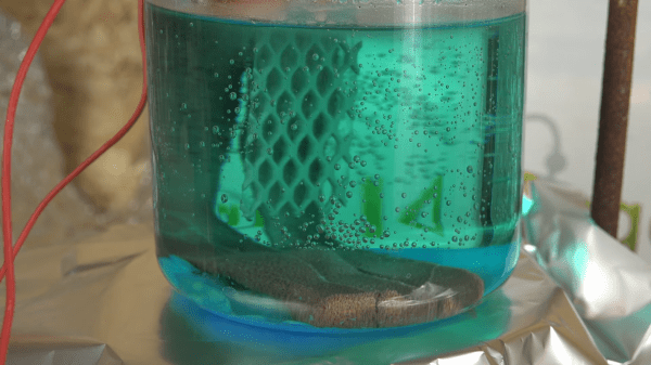
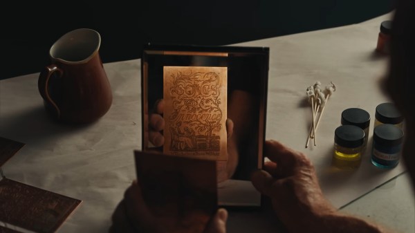
Blake sought to marry his art with his poetry and unleash it on the world. To do so, he created an innovative printing process, which is recreated by [Michael Phillips] in the video after the break. Much like etching a PCB, Blake started with a copper sheet, writing and drawing his works backwards with stopping varnish, an acid-resistant varnish that sticks around after a nitric acid bath. The result was a raised design that could then be used for printing.

Cleaning up the ink smudges before printing.

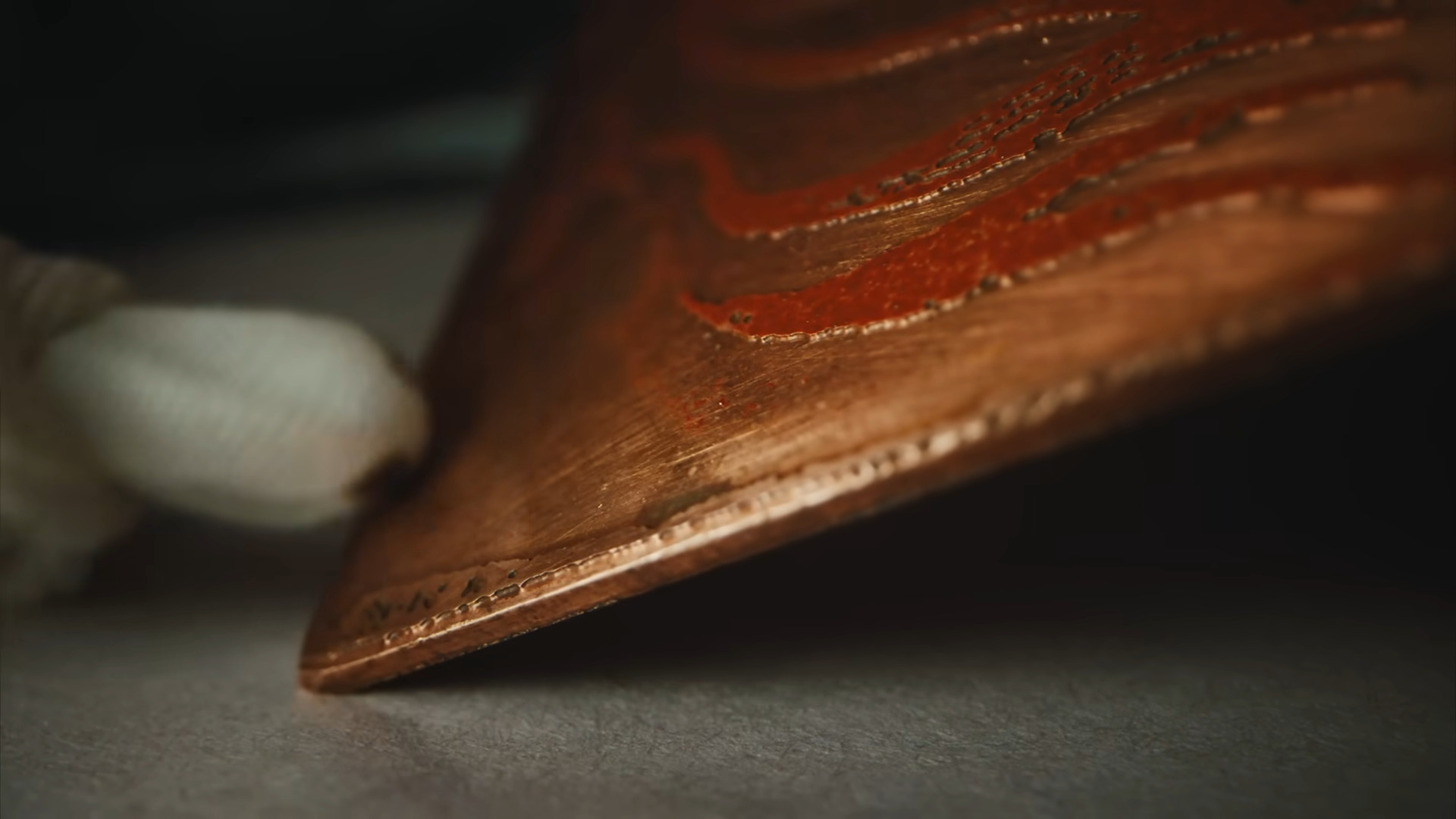
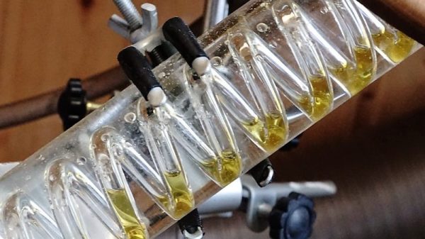
Blake was a master of color, using few pigments plus linseed or nut oil to create pastes of many different hues. Rather than use a brayer, Blake dabbed ink gently around the plate, careful not to splash ink or get any in the etched-away areas. As this was bound to happen anyway, Blake would then spend more time wiping out the etched areas than he did applying the ink.

Another of Blake’s innovations was the printing process itself. Whereas traditionally, illuminated texts must be printed in two different workshops, one for the text and the other for the illustrations, Blake’s method of etching both in the same plate of copper made it possible to print using his giant handmade press.

Want to avoid censorship and print your own ‘zines? Why not build a proofing press?.

Continue reading “William Blake Was Etching Copper In 1790”

Scanning electron micrograph of a microfabricated lens array

Getting A Fly’s-Eye View With Microfabricated Lens Arrays

Atomic force microscopy, laser ablation, and etching with a witches brew of toxic chemicals: sounds like [Zachary Tong] has been playing in the lab again, and this time he found a way to fabricate arrays of microscopic lenses as a result.

Like many of the best projects, [Zach]’s journey into micro-fabrication started with a happy accident. It happened while he was working on metal-activated chemical etching (MACE), which uses a noble metal catalyst to selectively carve high-aspect-ratio features in silicon. After blasting at a silver-coated silicon wafer with a laser, he noticed the ablation pits were very smooth and uniform after etching. This led him to several hypotheses about what was going on, all of which he was able to test.

The experiments themselves are pretty interesting, but what’s really cool is that [Zach] realized the smooth hemispherical pits in the silicon could act as a mold for an array of microscopic convex lenses. He was able to deposit a small amount of clear silicone resin into the mold by spin-coating, and (eventually) transfer the microlens array to a glass slide. The lenses are impressively small — hundreds of them over only a couple hundred square microns — and pretty well-formed. There’s always room for improvement, of course, but for an initial attempt based on a serendipitous finding, we’d call it a win. As for what good these lenses are, your guess is as good as ours. But novel processes like these tend to find a way to be useful, and the fact that this is coming out of a home lab doesn’t change that fact.

We find this kind of micro-fabrication fascinating. Whether it’s making OLED displays, micro-machining glass with plasma, or even rolling your own semiconductors, we can’t get enough of this stuff.

Continue reading “Getting A Fly’s-Eye View With Microfabricated Lens Arrays”

Recovering Metal From Waste

Refining precious metals is not as simple as polishing rocks that have been dug out of the ground. Often, complex chemical processes are needed to process the materials properly or in high quantities, but these processes leave behind considerable waste. Often, there are valuable metals left over in these wastes, and [NerdRage] has gathered his chemistry equipment to demonstrate how it’s possible to recover these metals.

The process involved looks to recover copper and nitric acid from copper nitrate, a common waste byproduct of processing metal. While a process called thermal decomposition exists to accomplish this, it’s not particularly efficient, so this alternative looks to improve the yields you could otherwise expect. The first step is to react the copper nitrate with sulfuric acid, which results in nitric acid and copper sulfate. From there, the copper sulfate is placed in an electrolysis cell using a platinum cathode and copper anodes to pass current through it. After the process is complete, all of the copper will have deposited itself on the copper electrodes.

The other interesting thing about this process, besides the amount of copper that is recoverable, is that the sulfuric acid and the nitric acid are recoverable, and able to be used again in other processes. The process is much more efficient than thermal decomposition and also doesn’t involve any toxic gasses either. Of course, if collecting valuable metals from waste is up your alley, you can also take a look at recovering some gold as well.

Thanks to [Keith] for the tip!

Continue reading “Recovering Metal From Waste”

Learn IC Decapping

Decapsulating ICs used to be an exotic technique. (I should know, I did that professionally for one of the big IC vendors back in the 1980s.) These days, more and more people are learning to take apart ICs for a variety of reasons. If you are interested in doing it yourself, [Juan Carlos Jimenez] has a post you should read about using acid to remove epoxy from ICs.

[Juan Carlos] used several different techniques with varying degrees of success. Keep in mind, that using nitric acid is generally pretty nasty. You need safety equipment and be sure to plan for bad things to happen. Have eyewash ready because once you splash acid in your eye, it is too late to get that together.

Continue reading “Learn IC Decapping”

Anyone Need A Little Fuming Nitric Acid?

If there’s a chemical with a cooler name than “fuming nitric acid,” we can’t think of it. Nearly pure nitric acid is useful stuff, especially if you’re in the business of making rocket fuels and explosives. But the low-end nitric acid commonly available tops out at about 68% pure, so if you want the good stuff, you’ll have to synthesize fuming nitric acid yourself. (And by “good stuff”, we mean be very careful with the resulting product.)

Fuming nitric acid comes in two colors – red fuming nitric acid (RFNA), which is about 90% pure and has some dissolved nitrogen oxides, giving it its reddish-brown color. White fuming nitric acid (WFNA) is the good stuff — more than 99% pure. Either one is rough stuff to work with — you don’t want to wear latex or nitrile gloves while using it. It’s not clear what [BarsMonster] needs the WFNA for, although he does mention etching some ICs. The synthesis is pretty straightforward, if a bit dangerous. An excess of sulfuric acid is added to potassium nitrate, and more or less pure nitric acid is distilled away from the resulting potassium sulfate. Careful temperature control is important, and [BarsMonster] seems to have gotten a good yield despite running out of ice.

We don’t feature too many straight chemistry hacks around here, but this one seemed gnarly enough to be interesting. We did have a Hackaday Prize entry a while back on improvements to the Haber process for producing ammonia, which curiously is the feedstock for commercial nitric acid production processes.

Continue reading “Anyone Need A Little Fuming Nitric Acid?”

Taking A Look At Decapped ICs

Aside from wanting to play around with nitric acid, [Ben] really didn’t have a reason to decap a few 74xx and 4000-series logic chips. Not that we mind, as he provides a great tutorial at looking at a bare IC that isn’t covered in epoxy and resin.

Most ICs are encased in a hard epoxy shell making it very difficult to look at the circuits within. [Ben] tried to grind this epoxy off with a Dremel tool, but didn’t have much luck until he moved over to a CNC mill to remove 0.040 – 0.050″ of epoxy without breaking the bond wires.

After carving out a nice pocket above the die, [Ben] put a few drops of nitric acid on the chip to dissolve the epoxy coating.  This worked very slowly at room temperature, but after putting the chips on a hot plate the acid was able to reveal the die underneath.

After successfully removing all the epoxy and giving them an acetone bath, [Ben] took his chips over to the microscope and was able to check out the underlying circuit. He doesn’t have any idea what he could do with these decapped logic chips, but the bond wires are still intact so he could still use these chips in a build.

We’d like to see a few decapped MEMS devices, but if you have a suggestion on what [Ben] can do with his decapped chips, drop a note in the comments.

Continue reading “Taking A Look At Decapped ICs”

Decapping Integrated Circuits With Sap

[James] is interested in reverse engineering some integrated circuits. One of the biggest hurdles in this process has always been just getting to the guts of the chip. He used acetone to dissolve the plastic case but had trouble getting through the epoxy blob. Commonly, the epoxy is soaked in nitric acid for a few minutes but [James] didn’t have access to that chemical. Instead he popped into the local music store and picked up some rosin (used to make violin bows sticky enough to grab the strings of the instrument). After boiling down the rock-hard rosin and the chip for 20 minutes, he got a clean and relatively undamaged semiconductor that he can easily peer into.