You may not think much of origami or its cousin-with-cutouts kirigami, but the latter could (and already is) helping to save the planet. But let’s back up a bit.
Most readers will be familiar with origami, the Japanese art of folding paper. But there is also kirigami, which uses a series of cuts to produce 3D shapes from 2D stock. Turns out that if you cut paper just right, you can turn it into highly-recyclable packaging that even interlocks with itself, negating the need for folding or even tape.
 The video after the break takes a look at 3M’s Scotch Cushion Lock™ protective wrap through the eyes of its inventor, Tom Corrigan. It all started when 3M wanted to create a self-assembling box from a flat piece of cardboard.
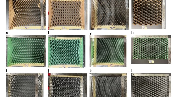
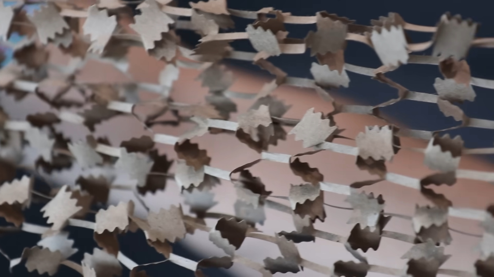
So far, that particular invention hasn’t come to fruition, but after many long nights with paper and X-Acto knives, Tom came up with a honeycomb design with strong vertical walls that absorb energy much like bubble wrap or packing peanuts. The toothiness of each honeycomb wall adds height which adds strength, and allows the packaging to interlock with itself.
Not only is this packaging easier to recycle, it takes up way less space than other packaging alternatives. Once expanded, a 1,000 square foot roll of this stuff is equal to 2,500 square feet of bubble wrap, which constitutes about a dozen rolls.
Now, what to do about all that expanded polystyrene packaging still out there? With the right tool, you can turn it into insulation.
Continue reading “Saving The Planet With Carefully Cut Paper”