For the next post in the Creating A PCB series, we’re going to continue our explorations of Eagle. In Part 1, I went over how to create a part from scratch in Eagle. In Part 2, we used this part to create the small example board from the Introduction.
This time around I’ll be going over Design Rule Check (DRC) — or making sure your board house can actually fabricate what you’ve designed. I’ll also be covering the creation of Gerber files (so you can get the PCB fabbed anywhere you want), and putting real art into the silkscreen and soldermask layers of your boards.
The idea behind this series is to explore different EDA suites and PCB design tools by designing the same circuit in each. You can check out the rest of the posts in this series right here.
In the last (and first) post in this series, we took a look at Eagle. Specifically, we learned how to create a custom part in Eagle. Our goal isn’t just to make our own parts in Eagle, we want to make schematics, boards, and eventually solder a few PCBs.
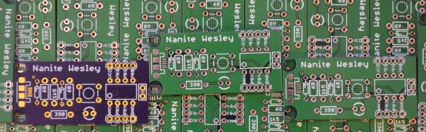
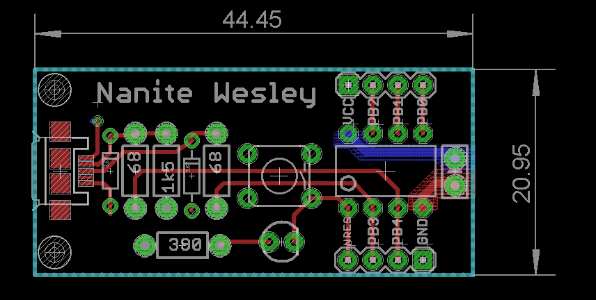
The board we’ll be making, like all of the boards made in this Creating A PCB In Everything series, is the Nanite Wesley, a small USB development platform based on the ATtiny85. This board has less than a dozen parts, most of which are through-hole. This is the simplest PCB I can imagine that has sufficient complexity to demonstrate how to make a board.
With that said, let’s get onto the second part of our Eagle tutorial and lay out our circuit board.
For the first in a series of posts describing how to make a PCB, we’re going with Eagle. Eagle CAD has been around since the days of DOS, and has received numerous updates over the years. Until KiCad started getting good a few years ago, Eagle CAD was the de facto standard PCB design software for hobbyist projects. Sparkfun uses it, Adafruit uses it, and Dangerous Prototypes uses it. The reason for Eagle’s dominance in a market where people don’t want to pay for software is the free, non-commercial and educational licenses. These free licenses give you the ability to build a board big enough and complex enough for 90% of hobbyist projects.
Of course, it should be mentioned that Eagle was recently acquired by Autodesk. The free licenses will remain, and right now, it seems obvious Eagle will become Autodesk’s pro-level circuit and board design software.
Personally, I learned PCB design on Eagle. After a few years, I quickly learned how limited even the professional version of Eagle was. At that point, the only option was to learn KiCad. Now that Eagle is in the hands of Autodesk, and I am very confident Eagle is about to get really, really good, I no longer have the desire to learn KiCad.
With the introduction out of the way, let’s get down to making a PCB in Eagle.
A few years ago, I wrote a few columns titled Making A Thing. These columns were a tutorial of sorts for several different 3D modeling programs. This column wasn’t meant to be a complete guide to modeling an object in OpenSCAD or SolidWorks, it was just step-by-step instructions on how to make one specific thing with one specific piece of software.
More than a few people in the Hackaday community found this column useful or at the very least an interesting pedagogical device. When starting out with any kind of productivity software, you don’t need to know how to do everything, you just need to know how to do the most common tasks.
Since the Making A Thing column was so popular, I felt it was time to revive this idea with another design task we often face. As you have already guessed, we’re going to be making printed circuit boards. Continuing the unique tutorial format created in the previous iteration of this column, Making a PCB will build one specific circuit in multiple EDA suites.
The Circuit
The entire concept of demonstrating how to build one thing in a specific software package necessitates a model thing. Before I even begin writing the first Making A PCB column, I need to design something that’s sufficiently complex but still relatively simple, and something that’s hopefully somewhat useful. Breakout boards are extremely simple, perhaps too much. In the course of these programs, I’ll need to demonstrate how to make a part in each specific software suite, so fewer pins are better.
Lacking any creativity of my own, I’ve settled on a very small ATtiny85 Arduino derivative from Tim a.k.a. [cpldcpu]. Tim’s Nanite 85 is an exceptionally small Arduino-compatible board based on the ATtiny85, complete with a USB port, LED, and a few pins of I/O. It’s simple but sufficiently complex to give an introduction to a PCB design suite.
I’m not going to outright copy Tim’s Nanite 85, though. It’s much clearer if parts aren’t stacked on top of each other, and I’d like to give myself a little breathing room on the layout. I’ve redesigned the circuit of the Nanite 85 to use mostly through-hole parts on a slightly larger board. I’m calling my version the Nanite Wesley, and if you get that reference, thumbs up for you.
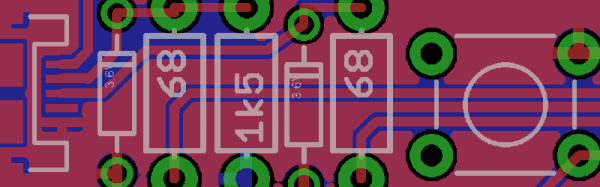
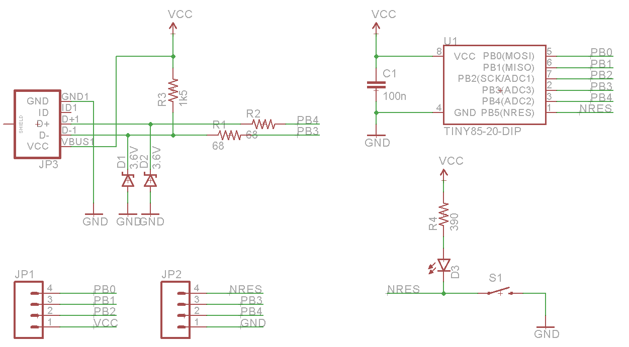
The schematic for the Nanite WesleyThe Nanite Wesley board. Copper pours not shown
Is this how a board should be laid out? No, absolutely not. I could probably do this as a single-layer board. This is a very inefficient layout, and I like rounded corners on my boards. It’s good enough, though, and it works. This is meant to be a tutorial on how to use a PCB design package, not a tutorial on how to design a PCB. Your criticisms in this regard are noted and ignored.
What These Tutorials Will Consist Of
You cannot use a PCB design package until you know how to make a part. Yes, Eagle has wonderful libraries for almost everything you can imagine, KiCad has plenty of parts on the Internet, and if you’re using a cloud-based PCB software, almost everything will be provided for you. If you make a PCB, eventually you’ll have to make your own part, though, and each tutorial will begin with making a DIP-8 ATtiny85. Everything else on this board is a jellybean part. Either way, the process of making a part and package for a Zener is the same as making one for a microcontroller.
The next part of the tutorial will consist of schematic capture. This means placing the parts in the schematic, drawing wires between the pins and pads, and naming them. From there, it’s time to actually make a board, and this means dropping the parts down, putting traces between all the pins, doing the board outline, pouring copper, and mechanical considerations.
With the schematic and board designed, it will be time to send it off to a fab house. For Eagle and KiCad, this is easy; OSHpark accepts Eagle .brd and KiCad .pcb files, but this is cheating. We’re going to use CAM to generate real Gerber files. If you make enough PCBs, you’ll have to learn it eventually.
Caveats and Poor Design
There are a lot of things that go into making a ‘proper’ PCB, including isolation, direct traces to decoupling capacitors, making sure pixies don’t go around sharp corners and a thousand other items that won’t be discussed in these tutorials. There’s a reason I won’t be discussing this. This is a guide on how to use a PCB design tool, not how to design a PCB.
What else should I do?
As you can probably guess from the schematic above, the first PCB software I’m going to cover is Eagle. KiCad is on the list, as is Fritzing, Altium CircuitMaker, and OrCAD. In the interests of putting PCB design in a historical context, I have a copy of AutoTRAX and an old DOS machine. I’ll also be covering a few of the cloud-only design tools such as Upverter.
That’s enough software suites to get started, but as with the Making A Thing series, I’m going to be looking for suggestions from the peanut gallery. I can’t change the circuit I’m making, as that’s the entire point of this series, but I am looking for suggestions on other tools to cover. What else can I do? Want me to grab a piece of copper clad board, sticker overlays, and some photostatic film? I can do that. Are you at a web-based EDA startup, and want some free advertising? Leave a note in the comments.
Thanks to our efforts to slowly improve the backend of Hackaday, you’ll be able to access all the Making A PCB In Everything posts from the series list below.
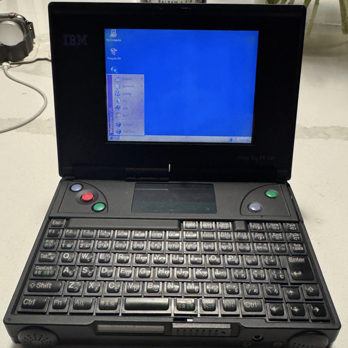
There’s a dedicated group of users out there that aren’t ready to let their beloved IBM PC110 go to that Great Big Data Center in the Sky. Unfortunately, between the limited available technical information and rarity of replacement parts, repairing the diminutive palmtops can be tricky.
Which is why [Ahmad Byagowi] has started a project that aims to not only collect all the available schematics and datasheets that pertain to the machine, but to reverse engineer all of the computer’s original circuit boards. Working from optical and x-ray scans, the project has already recreated the motherboard, power supply, modem, keyboard, and RAM module PCBs in KiCad.
Just last week the project released production-ready Gerbers for all the boards, but considering there have been 45+ commits to the repository since then, we’re going to assume they weren’t quite finalized. Of course, with a project of this magnitude, you’d expect it to take a few revisions to get everything right. (Hell, we’ve managed to screw up board layouts that had fewer than a dozen components on them.)
If you’d like to lend a hand, [Ahmad] says he could use the help. Beyond checking the boards for problems and reporting issues, he’s also on the hunt for any datasheets or other documentation that can be found for the PC110 or its components. It looks like there’s still schematic work that needs to be done as well, so if your idea of zen is figuring out how ~30 year old computers were wired up internally, this might be the perfect summer project for you.
Interestingly, our very own [Arya Voronova] has been working on creating a drop-in replacement motherboard for the Sony Vaio P using KiCad and imported board images. That hobbyists are now able to do this kind of work using free and open source tools is a reminder of just how far things have come in the last few years.
Backing up. It’s such a simple thing on paper – making a copy of important files and putting them in a safe place. In reality, for many of us, it’s just another thing on that list of things we really ought to be doing but never quite get around to.
I was firmly in that boat. Then, when disaster struck, I predictably lost greatly. Here’s my story on what I lost, what I managed to hang on to, and how I’d recommend you approach backups starting today.
“LEDs improve everything.” Words to live by. Most everything that Debra Ansell of [GeekMomProjects] makes is bright, bold, and blinky. But if you’re looking for a simple string of WS2812s, you’re barking up the wrong tree. In the last few years, Debra has been making larger and more complicated assemblies, and that has meant diving into the mechanical design of modular PCBs. In the process Debra has come up with some great techniques that you’ll be able to use in your own builds, which she shared with us in a presentation during the 2021 Hackaday Remoticon.
She starts off with a quick overview of the state of play in PCB art, specifically of the style that she’s into these days: three dimensional constructions where the physical PCB itself is a sculptural element of the project. She’s crossing that with the popular triangle-style wall hanging sculpture, and her own fascination with “inner glow” — side-illuminated acrylic diffusers. Then she starts taking us down the path of creating her own wall art in detail, and this is where you need to listen up. Continue reading “Remoticon 2021 // Debra Ansell Connects PCB In Ways You Didn’t Expect”→