As computers have gotten smaller and less expensive over the years, so have their components. While many of us got our start in the age of through-hole PCBs, this size reduction has led to more and more projects that need the use of surface-mount components and their unique set of tools. These tools tend to be more elaborate than what would be needed for through-hole construction but [Tobi] has a new project that goes into some details about how to build surface-mount projects without breaking the bank.
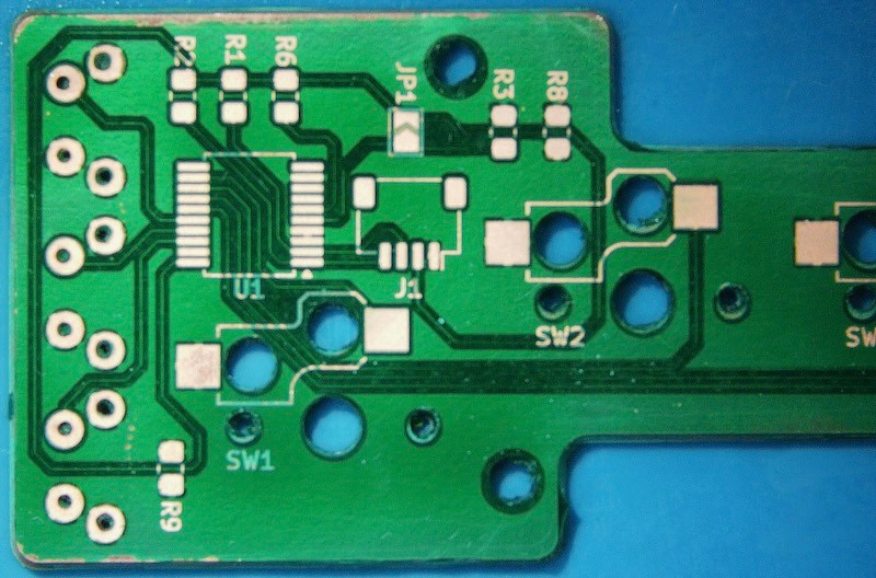
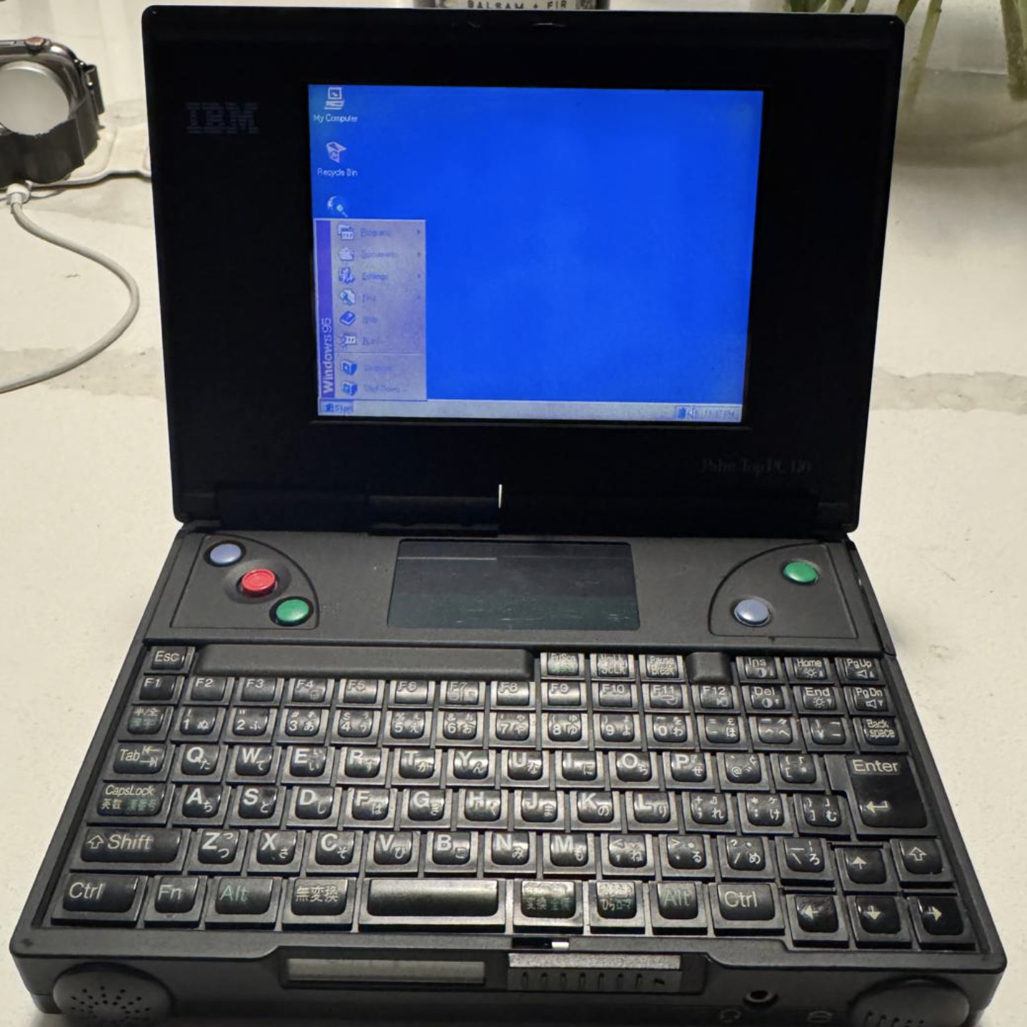
The project here is interesting in its own right, too: a display module upgrade for the classic Game Boy based on an RP2350B microprocessor. To get all of the components onto a PCB that actually fits into the original case, though, surface-mount is required. For that [Tobi] is using a small USB-powered hotplate to reflow the solder, a Pinecil, and a healthy amount of flux. The hotplate is good enough for a small PCB like this, and any solder bridges can be quickly cleaned up with some extra flux and a quick pass with a soldering iron.
The build goes into a lot of detail about how a process like this works, so if you’ve been hesitant to start working with surface mount components this might be a good introduction. Not only that, but we also appreciate the restoration of the retro video game handheld complete with some new features that doesn’t disturb the original look of the console. One of the other benefits of using the RP2350 for this build is that it’s a lot simpler than using an FPGA, but there are perks to taking the more complicated route as well.
Continue reading “Game Boy PCB Assembled With Low-Cost Tools”