Write In PipelineC For FPGAs

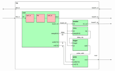
The best thing about field-programmable gate arrays (FPGAs), when you have a massively parallel application, is that everything runs in parallel. The worst thing about FPGAs, when you need a lot of stuff to happen in sequence, is that everything runs in parallel. If you have a multi-step computation, for example, you need to break it up into chunks, figure out the timing between them, and make sure that each chunk clears before it is fed new data. This is pipelining, and taking care of all the low-level details yourself is one of the things that can sometimes make FPGA a four-letter word beginning with “F”.

[Julian Kemmerer]’s PipelineC is a C-like language that compiles down into VHDL so that you can use it in an FPGA, and it does the pipelining for you. He has examples of how you’d use it to construct a simple state machine, and after you’ve written a few hundred state machines the long way, you’ll know why this is a good idea.

PipelineC isn’t the only high level synthesis language out there, but it sits in an interesting place. It doesn’t take care of memory or define interfaces. It just takes care of pipelining. We haven’t tried it out yet, but it looks like it would be interesting for moderately complex projects, where the mechanics of pipeline signalling is a hassle, but you don’t require the deluxe treatment. Check it out, and if you like it, let us (and [Julian], natch) know.

If you want to dive head-first into pipelining, give [Al Williams]’ two-part mini-series a look.

Pipeline graphic CC BY-SA 3.0 by CBurnett

Glasgow Uses An FPGA As An Embedded Systems Multitool

Everyone who builds embedded systems wants tools to help build and debug systems faster, so it isn’t uncommon to see boards outfitted with various tools like serial port sniffers. We’ve seen a few incarnations and the latest is Glasgow. The small board uses an FPGA and claims to do the following:

  • UART with automatic baud rate determination
  • SPI or I2C
  • Read and write common EEPROMs and flash chips
  • Read and write common EPROMs including a data rescue function
  • Program AVR chips via SPI
  • Play back JTAG SVF files
  • Debug ARC and some MIPS CPUs
  • Program XC9500LX CPLDs
  • Communicate to several wireless radios and CPUs
  • Do sound synthesis
  • Read raw data from floppy drives

The revC board is the first to be relatively functional and sports 16 I/O pins operating at up to 100 MHz, although the documentation hints that 6 MHz might be the top of what’s easily accomplished. The software is written in Python and the iCE40 FPGA toolchain that we’ve talked about many times in the past.

This already looks like a useful tool and the reconfigurable nature of FPGAs makes it a good platform to expand. The documentation discusses the difficulty in debugging things for the board, so the base software offers support such as a built-in logic analyzer to help.

We have seen dev boards become bench tools, like using the iCEstick as a logic analyzer. It’s nice to see dedicated tools like this one built up around the speed and versatility of FPGAs.

Continue reading “Glasgow Uses An FPGA As An Embedded Systems Multitool”

Lattice Drops EULA Clause Forbidding FPGA Bitstream Reverse Engineering

Yesterday we reported that Lattice Semiconductor had inserted a clause that restricted the reverse engineering of bitstreams produced by their FPGA toolchains. Although not explicitly stated, it’s assumed that this was directed toward several projects over the past five years that have created fully open source toolchains by reverse engineering the bitstream protocols of the Lattice ICE40 and ECP5 FPGA architectures. Late yesterday Lattice made an announcement reversing course.

To the open source community, thank-you for pointing out a new bitstream usage restriction in the Lattice Propel license. We are excited about the community’s engagement with Lattice devices and our intent is to not hinder the creation of innovative open source FPGA tools.

It’s refreshing then to see this announcement from Lattice Semiconductor. Even more so is the unexpected turn of speed with which they have done so, within a couple of days of it being discovered by the open-source community. We report depressingly often on boneheaded legal moves from corporations intent on curbing open source uses of their products. This announcement from Lattice removes what was an admonition opposing open source toolchains, can we hope that the company will continue yesterday’s gesture and build a more lasting relationship with the open source community?

The underlying point to this story is that in the world of electronics there has long been an understanding that hardware hackers drive product innovation which will later lead to more sales. Texas Instruments would for years supply samples of exotic semiconductors to impecunious students for one example, and maybe you have a base-model Rigol oscilloscope with a tacitly-approved software hack that gives it an extra 50MHz of bandwidth for another.

We can only congratulate Lattice on their recognition that open source use of their products is beneficial for them, and wish that some of the other companies triggering similar stories would see the world in the same way. Try interacting more with your open source fans; they know and love your hardware more than the average user and embracing that could mean a windfall for you down the road.

An Open Source HDMI Implementation For FPGAs

With some clever hacks and fast IO work, it’s possible to get your average garden-variety microcontroller to output some form of video. Old analog standards like composite and VGA are just slow enough that it’s possible to bitbash one’s way to success. If you’re serious about video work, however, you’ll want something more capable. For those use cases, [purisame]’s got what you need – an open source HDMI implementation for FPGAs.

Unlike other free and open source projects in this space, [purisame] has eschewed simply outputting compatible DVI signals on the port. This implementation is pure HDMI 1.4b, enabling the extended capabilities this brings, like combined video and audio streams. Thus far, it’s been tested on Xilinx and Altera platforms, though it may be compatible with Lattice, too.

In addition to the code, [purisame] breaks down options for those looking at going into production with an HDMI device. Licencing the technology for sale can be a fraught area, so a lawyer is recommended if you’re heading to market. Oh, and funnily enough, if your really do want to do HDMI on an Arduino, there’s a shield for that, too. Natch!

FPGA Raises Component Video From A Sinclair ZX Spectrum

An abiding memory of the early-80s heyday of 8-bit computing for many is operating their computer from the carpet in front of the family TV. While the kids in the computer adverts had parents who bought them a portable colour telly on which to play Jet Set Willy, the average kid had used up all the Christmas present money on the computer itself. The cable would have been an RF connection to the TV antenna socket, and the picture quality? At the time we thought it was amazing because we didn’t know any different, but with the benefit of nearly 40 years’ hindsight, it was awful.

For ZX Spectrum owners in 2020 a standard modification is to bring out a composite video signal, but [c0pperdragon] has gone a step or two beyond that with a component video interface. And this isn’t a mod in which the signals are lifted from the Spectrum’s colour encoder circuitry, instead it uses an FPGA hooked directly to the ULA chip to generate the component video itself.

The Altera chip sits on a little PCB designed to occupy the footprint of the original Astec modulator, and sports a neat bundle of wires hooked up to the various Spectrum signals it needs. There are a couple of jumpers to select the output type and resolution, it supports YPbPr or RGsB outputs and both 288p and 576p. If you think perhaps it looks a little familiar, that’s because it’s the sister project of an earlier board for the Commodore 64. So if you have a Spectrum and are annoyed by UHF and PAL, perhaps it’s worth a look.

All Your Passwords Are Belong To FPGA

When used for cracking passwords, a modern high-end graphics card will absolutely chew through “classic” hashing algorithms like SHA-1 and SHA-2. When a single desktop machine can run through 50+ billion password combinations per second, even decent passwords can be guessed in a worryingly short amount of time. Luckily, advanced password hashing functions such as bcrypt are designed specifically to make these sort of brute-force attacks impractically slow.

Cracking bcrypt on desktop hardware might be out of the question, but the folks over at [Scattered Secrets] had a hunch that an array of FPGAs might be up to the task. While the clock speed on these programmable chips might seem low compared to a modern CPUs and GPUs, they don’t have all that burdensome overhead to contend with. This makes the dedicated circuitry in the FPGA many times more efficient at performing the same task. Using a decade-old FPGA board intended for mining cryptocurrency, the team was able to demonstrate a four-fold performance improvement over the latest generation of GPUs.

An earlier version of the FPGA cracker

After seeing what a single quad FPGA board was capable of, the [Scattered Secrets] team started scaling the concept up. The first version of the hardware crammed a dozen of the ZTEX FPGA boards and a master control computer computer into a standard 4U server case. For the second version, they bumped that up to 18 boards for a total of 72 FPGAs, and made incremental improvements to the power and connectivity systems.

Each 4U FPGA cracker is capable of 2.1 million bcrypt hashes per second, while consuming just 585 watts. To put that into perspective, [Scattered Secrets] says you’d need at least 75 Nvidia RTX-2080Ti graphics cards to match that performance. Such an array would not only take up a whole server rack, but would burn through a staggering 25 kilowatts. Now might be a good time to change your password to something longer, or finally get onboard with 2FA.

We’ve covered attempts to reverse engineer hardware designed for cryptocurrency mining, but those were based around application-specific integrated circuits (ASICs) which by definition are very difficult to repurpose. On the other hand, disused FPGA-based miners offer tantalizing possibilities; once you wrap your mind around how they work, anyway.

[Thanks to Piejoe for the tip.]

Using An FPGA To Glitch The Olimex LPC-P1343

After trying out hardware hacking using an FPGA to interface with target hardware, [Grazfather] was inspired to try using the iCEBreaker (one of the many hobbyist FPGAs to have recently flooded the market) to build a UART-controllable glitcher for the Olimex LPC-P1343.

FPGA Modules (The cmd module intercepts what the host computer sends over UART, the resetter holds the reset line until the target is reset, the delay starts counting on reset and waits for a configured number of cycles before sending its signal, the trigger waits for the delay to finish before telling the pulse module to send a pulse, and the pulse works similar to the delay module and outputs to the power multiplexer.)

When the target board boots up, the bootROM reads the flash and determines whether the UART goes to a shell and if the shell can be used to read out the flash. This is meant for developing firmware and debugging it in the bootloader, only flashing a version when the firmware is production-ready. The vulnerability is that only a specific value read from address 0x2FC and the state of a few pins can lock the bootloader in the expected way, and any other value at the address causes the bootROM to consider the device unlocked. Essentially, the mechanism is the opposite of how a lock ought to work.

The goal is to get the CPU to misread the flash at the precise moment it is meant to be reading the specific value, then jumping to the bootloader in the unlocked state. The FPGA can be used as a tool between the host machine and target board, communicating via UART. The FGPA can support configuring the delay between resetting the target board and pulsing a ‘glitch voltage’, as well as resetting the target board and activating the glitch. The primary reasons for using the FPGA over a different microcontroller are that the FPGA allows for precise timing (83.3ns precision) and removes worries about jitters (a Raspberry Pi might have side effects from OS scheduling and other processes and microcontrollers might have interrupts messing up the timing).

The logic analyzer view

To simulate the various modules, [Grazfather] used Icarus Verilog as well as GTKWave to observe the waveforms generated. A separate logic analyzer observes the effects on real hardware.

With enough time, it is possible to brute force any combination of delay and width until you get a dump of the flash you’re not meant to read. You can check out how the width of the pulse gets wider until the max, when the delay is incremented and the width values are tried again.

Continue reading “Using An FPGA To Glitch The Olimex LPC-P1343”