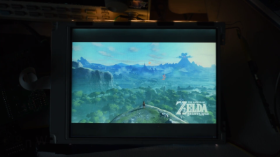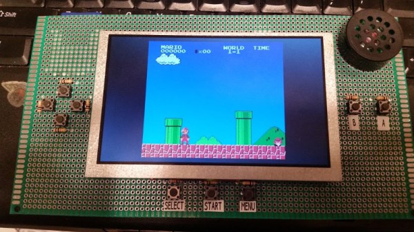
Usually when writing emulation software for a system like the Game Boy, one makes sure to take as many shortcuts as possible in order to reduce the resources required for the emulation. This has however the unfortunate side-effect that it reduces the overall accuracy of the emulation and with it the compatibility with games on the system.
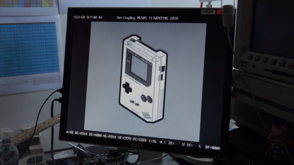
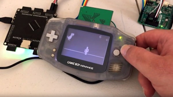
This is the basic reasoning behind projects which seek to abandon simplistic abstractions in favor of cycle-accurate, full compatibility approaches, of which MetroBoy is probably the most extreme one. Instead of abstracting away the hardware, it instead does the emulation at the circuit level. As with such other projects, this means that the emulator requires a lot more CPU cycles to get things just right. On the bright side, one can likely still run this emulator on any modern system.
As the MetroBoy author explains, he implemented code in C++ which allowed him to construct circuits in an HDL-style manner, which should theoretically also allow him to generate a Verilog (or VHDL) softcore out of the project. As a demonstration of implementing HDL in C++ it’s decidedly interesting.
An approach like this is pretty much the exact opposite of a project like the UltraHLE (ultra high-level emulator) Nintendo 64 emulator, which used the knowledge that Nintendo 64 games are written in C as a first step to creating libraries that the code in the Nintendo 64 ROMs would call instead of the native (Nintendo) libraries. This allowed N64 games to directly run on the target system, with the graphic and system calls translated by UltraHLE into native OS calls, using the 3dfx Glide API for accelerated graphics.
While an approach like UltraHLE took allows for the most minimal use of system resources by essentially foregoing emulation completely, for retro systems like the Game Boy where games were implemented in assembly on bare hardware, using this circuit-level emulation ensures that one gets the most accurate match with the original handheld console experience.
As a word of caution to those who are now itching to try out MetroBoy, its Github site notes that it currently lacks support for game saves, uses a mixture of original Game Boy (DMG) and Game Boy Advance SP (AGS) hardware that confuses some games and has rather buggy sound support.
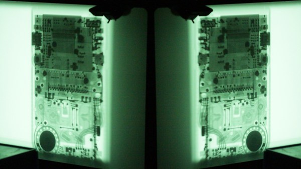
If playing around with software-defined Game Boy circuits isn’t enough and would like to literally look inside a real Game Boy, the X-ray image from the top of the article is something Chris over at Elektronaut pulled off several years ago.