Alright, here’s your quick and dirty hack for the day. The astute among you may recall [Peter Waldraff]’s bookshelf train build of a few days ago, and the fact that he used a switch made from a dead ballpoint pen to light up the scene. Fortunately, [Peter] wrote in to give us the details of this low-voltage sub-build, which you can see in the video after the break.
Essentially, [Peter] starts by making a shortened version of the pen. He modifies nearly every bit of it, including cutting down the ink cartridge, so if you try this, make sure the thing is all dried up first. Then, as he is screwing the point holder back on the barrel, he wraps elastic cord around the inside barrel in lieu of having sewing thread lying around. This cord along with some hot glue will hold a pair of paper clips to the sides of the point holder. When the pen is clicked into the writing position, it makes a connection between the paper clips and closes the circuit on whatever is wired into it.
What types of little hacks like this have gotten you through the build? Let us know in the comments, or better yet, write it up and drop us a tip. By the way, here is that bookshelf train build in case you missed it.
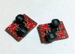 However, for some, switching regulators might look a bit intimidating. They tend to have higher standards for board layout compared to linear regulators, and, they do need an inductor – sometimes, a few more components too. Inductors alone are somewhat intimidating components, with a fair few more parameters than we’d expect, and you might get confused when looking into adding a switching regulator to your circuit.