MiSTER Multisystem 2 on a wooden table

MiSTer For Mortals: Meet The Multisystem 2

If you’ve ever squinted at a DE10-Nano wondering where the fun part begins, you’re not alone. This review of the Mr. MultiSystem 2 by [Lee] lifts the veil on a surprisingly noob-friendly FPGA console that finally gets the MiSTer experience out of the tinker cave and into the living room. Developed by Heber, the same UK wizards behind the original MultiSystem, this follow-up console dares to blend flexibility with simplicity. No stack required.

It comes in two varieties, to be precise: with, or without analog ports. The analog edition features a 10-layer PCB with both HDMI and native RGB out, Meanwell PSU support, internal USB headers, and even space for an OLED or NFC reader. The latter can be used to “load” physical cards cartridge-style, which is just ridiculously charming. Even the 3D-printed enclosure is open-source and customisable – drill it, print it, or just colour it neon green. And for once, you don’t need to be a soldering wizard to use the thing. The FPGA is integrated in the mainboard. No RAM modules, no USB hub spaghetti. Just add some ROMs (legally, of course), and you’re off.

Despite its plug-and-play aspirations, there are some quirks – for example, the usual display inconsistencies and that eternal jungle of controller mappings. But hey, if that’s the price for versatility, it’s one you’d gladly pay. And if you ever get stuck, the MiSTer crowd will eat your question and spit out 12 solutions. It remains 100% compatible with the MiSTer software, but allows some additional future features, should developers wish to support them.

Want to learn more? This could be your entrance to the MiSTer scene without having to first earn a master’s in embedded systems. Will this become an alternative to the Taki Udon announced Playstation inspired all-in-one FPGA console? Check the video here and let us know in the comments. Continue reading “MiSTer For Mortals: Meet The Multisystem 2”

Mainboard with the two 128 kB EPROMs containing the special MacIntosh Plus ROM image. (Credit: Pierre Dandumont)

The Lost 256 KB Japanese ROM For The Macintosh Plus Has Been Found

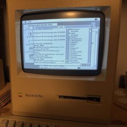
The Apple Macintosh Plus was one of the most long-lived Apple computers and saw three revisions of its 128 kB-sized ROMs during its life time, at least officially. There’s a fourth ROM, sized 256 kB, that merges the Western ROMs with Japanese fonts. This would save a user of a Western MacIntosh Plus precious start-up time & RAM when starting software using these fonts. Unfortunately, this particular ROM existed mostly as a kind of myth, until [Pierre Dandumont] uncovered one (machine-translated, French original).

The two 128 kB EPROMs containing the special MacIntosh Plus ROM image. (Credit: Pierre Dandumont)

Since this particular ROM was rumored to exist somewhere in the Japanese market, [Pierre] went hunting for Japanese Macintosh Plus mainboards, hoping to find a board with this ROM. After finally getting lucky, the next task was to dump the two 128 kB EPROMs. An interesting sidenote here is that the MacIntosh Plus’ two ROM sockets use the typical programming voltage pin (Vpp) as an extra address line, enabling 256 kB of capacity across the two sockets.

This detail probably is why this special ROM wasn’t verified before, as people tried to dump them without using that extra address line, i.e. as a typical 27C512 64 kB EPROM instead of this proprietary pinout, which would have resulted in the same 64 kB dump as from a standard ROM. Thanks to [Doc TB]’s help and his UCA device it was possible to dump the whole image, with the images available for download.

Using this ROM image was the next interesting part, as [Pierre] initially didn’t have a system to test it with, and emulators assume the 128 kB ROM format. Fortunately these are all problems that can be solved, allowing the ROM images to be validated on real hardware as well as a modified MAME build. We were informed by [Pierre] that MAME releases will soon be getting support for this ROM as well.

Remembering More Memory: XMS And A Real Hack

Last time we talked about how the original PC has a limit of 640 kB for your programs and 1 MB in total. But of course those restrictions chafed. People demanded more memory, and there were workarounds to provide it.

However, the workarounds were made to primarily work with the old 8088 CPU. Expanded memory (EMS) swapped pages of memory into page frames that lived above the 640 kB line (but below 1 MB). The system would work with newer CPUs, but those newer CPUs could already address more memory. That led to new standards, workarounds, and even a classic hack.

XMS

If you had an 80286 or above, you might be better off using extended memory (XMS). This took advantage of the fact that the CPU could address more memory. You didn’t need a special board to load 4MB of RAM into an 80286-based PC. You just couldn’t get to with MSDOS. In particular, the memory above 1 MB was — in theory — inaccessible to real-mode programs like MSDOS.

Well, that’s not strictly true in two cases. One, you’ll see in a minute. The other case is because of the overlapping memory segments on an 8088, or in real mode on later processors. Address FFFF:000F was the top of the 1 MB range.

PCs with more than 20 bits of address space ran into problems since some programs “knew” that memory access above that would wrap around. That is FFFF:0010, on an 8088, is the same as 0000:0000. They would block A20, the 21st address bit, by default. However, you could turn that block off in software, although exactly how that worked varied by the type of motherboard — yet another complication.

XMS allowed MSDOS programs to allocate and free blocks of memory that were above the 1 MB line and map them into that special area above FFFF:0010, the so-called high memory area (HMA). Continue reading “Remembering More Memory: XMS And A Real Hack”

Fancy Adding A Transputer Or Two To Your Atari ST?

Has anybody heard of the ATW800 transputer workstation? The one that used a modified Atari ST motherboard as a glorified I/O controller for a T-series transputer?  No, we hadn’t either, but transputer superfan [Axel Muhr] has created the ATW800/2, an Atari Transputer card, the way it was meant to be.

The transputer was a neat idea when it was conceived in the 1980s. It was designed specifically for parallel and scientific computing and featured an innovative architecture and dedicated high-speed serial chip-to-chip networking. However, the development of more modern buses and general-purpose CPUs quickly made it a footnote in history. During the same period, a neat transputer-based parallel processing computer was created, which leveraged the Atari ST purely for its I/O. This was the curious ATW800 transputer workstation. That flopped as well, but [Axel] was enough of a fan to take that concept and run with it. This time, rather than using the Atari as a dumb I/O controller, the card is explicitly designed for the Mega-ST expansion bus. A second variant of the ATW800/2 is designed for the Atari VME bus used by the STe and TT models—yes, VME on an Atari—it was a thing.

Continue reading “Fancy Adding A Transputer Or Two To Your Atari ST?”

Your Own Core Rope Memory

If you want read-only memory today, you might be tempted to use flash memory or, if you want old-school, maybe an EPROM. But there was a time when that wasn’t feasible. [Igor Brichkov] shows us how to make a core rope memory using a set of ferrite cores and wire. This was famously used in early UNIVAC computers and the Apollo guidance computer. You can see how it works in the video below.

While rope memory superficially resembles core memory, the principle of operation is different. In core memory, the core’s magnetization is what determines any given bit. For rope memory, the cores are more like a sensing element. A set wire tries to flip the polarity of all cores. An inhibit signal stops that from happening except on the cores you want to read. Finally, a sense wire weaves through the cores and detects a blip when a core changes polarity. The second video, below, is an old MIT video that explains how it works (about 20 minutes in).

Why not just use core memory? Density. These memories could store much more data than a core memory system in the same volume. Of course, you could write to core memory, too, but that’s not always a requirement.

We’ve seen a resurgence of core rope projects lately. Regular old core is fun, too.

Continue reading “Your Own Core Rope Memory”

RADUGA: The Retro Computer From Behind The Curtain

When [Kasyan] was six years old, he saw a RADUGA computer, a Russian unit from the 1990s, and it sparked his imagination. He has one now that is a little beat up, but we feel like he sees it through his six-year-old eyes as a shiny new computer. The computer, which you can see in the video below, was a clone of the Spectrum 48K.

The box is somewhat klunky-looking, and inside is also a bit strange. The power supply is a — for the time — state-of-the-art switching power supply. Since it wasn’t in good shape, he decided to replace it with a more modern supply.

The main board was also not in good shape. A Zilog CPU is on a large PCB with suspicious-looking capacitors. The mechanical keyboard is nothing more than a array of buttons, and wouldn’t excite today’s mechanical key enthusiast.

Continue reading “RADUGA: The Retro Computer From Behind The Curtain”

Remembering Memory: EMS, And TSRs

You often hear that Bill Gates once proclaimed, “640 kB is enough for anyone,” but, apparently, that’s a myth — he never said it. On the other hand, early PCs did have that limit, and, at first, that limit was mostly theoretical.

After all, earlier computers often topped out at 64 kB or less, or — if you had some fancy bank switching — maybe 128 kB. It was hard to justify the cost, though. Before long, though, 640 kB became a limit, and the industry found workarounds. Mercifully, the need for these eventually evaporated, but for a number of years, they were a part of configuring and using a PC.

Why 640 kB?

The original IBM PC sported an Intel 8088 processor. This was essentially an 8086 16-bit processor with an 8-bit external data bus. This allowed for cheaper computers, but both chips had a strange memory addressing scheme and could access up to 1 MB of memory.

In fact, the 8088 instructions could only address 64 kB, very much like the old 8080 and Z80 computers. What made things different is that they included a number of 16-bit segment registers. This was almost like bank switching. The 1 MB space could be used 64 kB at a time on 16-byte boundaries.

So a full address was a 16-bit segment and a 16-bit offset. Segment 0x600D, offset 0xF00D would be written as 600D:F00D. Because each segment started 16-bytes after the previous one, 0000:0020, 0001:0010, and 0002:0000 were all the same memory location. Confused? Yeah, you aren’t the only one.

Continue reading “Remembering Memory: EMS, And TSRs”