A few years ago, there was a rush of products on the market to detect motion. The idea being you could interact with your computer like they do on science fiction movies, with giant expressive hand motions in the air. Most of these were aimed at desktop computer users but one company, YouSpace, wanted to bring this technology to retail stores. [IMSAI Guy] got one of their sensor devices and decided to see what was inside it. You can see, too, in the video below.
The device appeared to have a laser inside, which motivated the teardown. We aren’t sure exactly what YouSpace had planned, but you can see their now-defunct website on the Wayback machine. The use cases listed didn’t really help us get a clear picture, so maybe that was part of the problem.
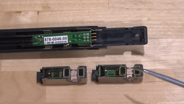
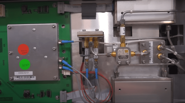
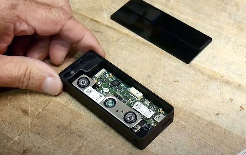 Getting into the device was the first challenge. Like many modern smartphones, there didn’t appear to be any fasteners, so you simply had to pry the case apart. Inside the case: a tiny circuit board and a metal assembly containing the laser and cameras that were easy to remove. The main PCB appears to be an Intel off-the-shelf board that was in many Intel RealSense products, and currently go for about $50 on eBay. The camera assembly looks a bit like an Intel D430, so it is possible the entire thing was off-the-shelf hardware. Even the little connector board is, technically, a D400 Interposer.
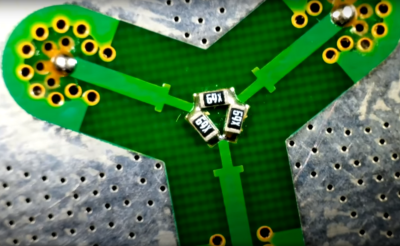
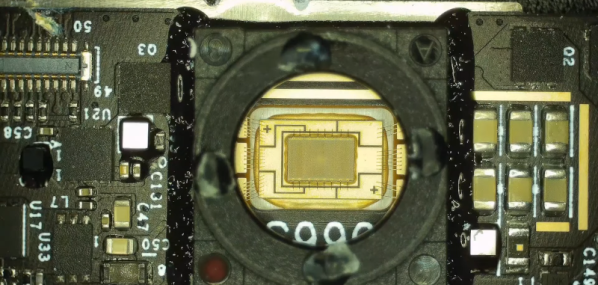
The peek into the structured light project under the microscope was interesting. We expected it would look different, and [IMSAI Guy] clearly didn’t expect its appearance either. The chip was made to beam a known pattern that the cameras would use to deduce the shape of the surfaces it hits.
If you can find these on the surplus market, they would probably be a good deal if you need this hardware which is typically pretty expensive. Just beware, though. Intel announced in late 2021 they were “winding down” RealSense. We don’t know if there will be third-party support in the future or if the whole product line will just be orphaned.
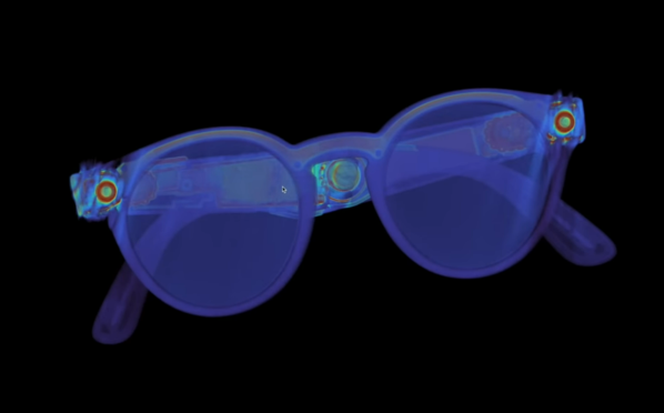
We’ve seen the occasional project that uses structured light. The technique can be very precise.
Continue reading “Gesture Sensor Teardown Reveals Intel Heritage”