These Wire Strippers Are Made From PCBs

The rise in cheap PCB fabrication has made old-school prototyping methods such as wire wrapping somewhat passé, but it still has its place. And if you’re going to wire wrap, you’re going to want a quick and easy way to strip that fine Kynar-insulated wire. So why not use PCB material to make this handy wire-wrapping wire stripper?

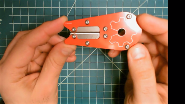
The tool that [danielrp] built is pretty simple – just a pair of razor blades held together so as to form a narrow slot to cut insulation while leaving the conductor untouched. The body of the tool is formed of two PCBs, between which the blades are sandwiched. [danielrp] designed the outline of the PCBs in DraftSight, then exported a DXF into EAGLE to make the Gerbers. The fabricated boards needed a little post-processing, including tapping the holes on one side to accept the screws that hold the tool together. We were surprised that FR4 took the threads at all, but it seems to work for this low-torque application. The disposable snap-type blades were sandwiched between the PCBs and the gap between them adjusted for nick-free stripping. The video below shows the design and build process.

We always appreciate homemade tools, and the fact that you can get a stack of PCBs for almost nothing makes us wonder what else we could use them for. We recently saw them used in a unique word clock, and even turned into a folding circuit sculpture.

Continue reading “These Wire Strippers Are Made From PCBs”

Building An Artisanal Tape Measure

Some tools are so common, so basic, that we take them for granted. A perfect example is the lowly tape measure. We’ve probably all got a few of these kicking around the lab, and they aren’t exactly the kind of thing you give a lot of thought to when you’re using them. But while most of us might not give our tape measure a second thought, [Ariel Yahni] decided to create an absolutely gorgeous new enclosure for his. Because if you’re going to measure something, why not look good doing it?

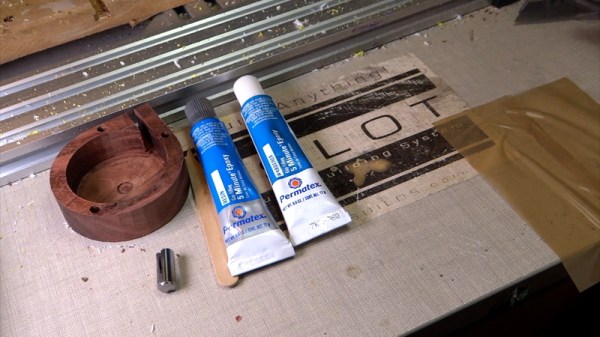
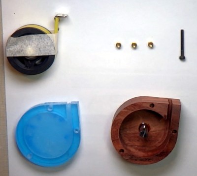
A CNC router is used to carve the body of the new tape measure out of a solid block of wood and cut a top plate out of clear acrylic. [Ariel] then used an angle grinder to cut off a small section of steel rod which he secured into a carved pocket in the base using epoxy. Finally, the internals of a commercial tape measure were inserted into this new enclosure, and the acrylic top was screwed down into place.

[Ariel] has made the DXF files for this project public for anyone else who wants to carve out their own heirloom tape measure, though it seems likely the designs will need some tweaking depending on the make and model of donor tape measure. While this might not be the most technically impressive project to run on Hackaday, it’s still a fantastic example of the sort of bespoke designs that are made possible with modern manufacturing methods.

This design reminds us of a similar project to turn a basic Honda key fob into a true conversation piece with the addition of some CNC’d hardwood and aluminum.

Continue reading “Building An Artisanal Tape Measure”

Homemade Test Jig Is Cheaper Than Outsourcing

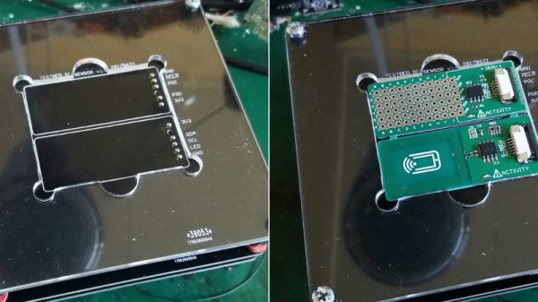
In the past, [Sjaak] has had his testing and programming jigs made for him in Shenzhen, but realized they weren’t that great of a value. They weren’t terribly expensive in the grand scheme of things, but they didn’t include any wiring, so he was still spending his own time and money. His quest to develop his own in-house jigs not only netted him a considerable cost savings in the end, but also produced a nicely detailed post on his site for anyone else who may be heading down the same path. That’s a win-win in our book.

The idea behind a jig is pretty simple: essentially it’s just a mount that holds the PCB, and a set of pins which contact the appropriate points on the board. The jig can then provide power, programming, status LEDs for testing, etc. Basically anything that you can’t or don’t want to include on the final board, but will help in testing or programming them.

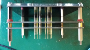
To start, [Sjaak] begins with a blank PCB in Eagle and imports his target board. With the two lined up, he can then mark where he wants the pins to go on the jig, and add labels to the silkscreen to make things a little easier during diagnostics. The target board is then removed, the file converted to Gerber, and it’s sent off for manufacturing. With a few more tweaks, the file is then exported to DXF and laser cut out of acrylic. When the PCBs come back, it’s just a matter of sandwiching it all together with some standoffs and adding the pins.

[Sjaak] mentions that he was inspired by an old post on how SparkFun was internally handling their test jigs, though we think with a dash of automation he could make things even easier for himself.

3D Printing With 2D Inkscape Projections

If you had a formal drafting class, you probably learned about making orthographic projections–engineering drawings with multiple views (for example, top, front, and right). Even if you didn’t take the class, you’ve probably seen drawings like this where you view a 3D object as a series of 2D views from different angles.

These days, you are more likely to create a 3D model of an object, especially if you are going to 3D print it. After all, the 3D printer software is going to expect a model. When [Nightshade] wanted a laptop stand for his workbench, he started trying to do a 3D model. His final product though, was made by creating two views in Inkscape. They aren’t exactly orthographic projections of the final product, but the idea is similar.

Inkscape is a vector graphics program and generally creates SVG files, although it can also save EPS files. [Nightshade] used pstoedit to convert the EPS output to DXF format. DXF files are still two dimensional, but OpenSCAD can extrude DXF files into 3D shapes.

Just having a 3D shape of one view isn’t sufficient, though. The OpenSCAD script rotates the objects to the correct orientation and intersects them to form the final object. This is different from the usual cases of using Inkscape to trace a scan or generate simple text.

Continue reading “3D Printing With 2D Inkscape Projections”

CERN Shows Off New KiCad Module Editor

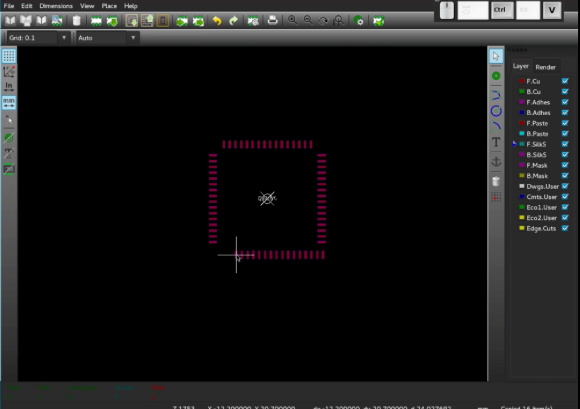
Photo from video demo of new KiCad module editor

CERN, the people that run a rather large particle collider, have just announced their most recent contributions to the KiCad project. This work focused on adding new features to the module editor, which is used to create footprints for parts.

The update includes support for DXF files, which will make it easy to import part drawings, or use external tools for more complex designs. New distribute tools make it easy to space out pads evenly. The copy and paste function now allows you to set a reference point, making it easy to align blocks. Finally, the pad enumeration tool lets you quickly set pin numbers.

CERN has already implemented a new graphics engine for KiCad, and demonstrated a new push and shove routing tool. The work plan for CERN’s KiCad contributions shows their long term goals. If you’re interested in what CERN is doing with KiCad, you can check out the CERN KiCad Developers Team on Launchpad.

After the break, watch a quick run through of the new features.

Continue reading “CERN Shows Off New KiCad Module Editor”

Make Any Shape Board In Eagle

circuit2

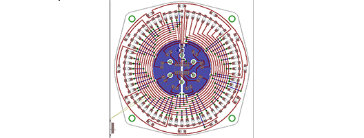
[Bryan] has been working on a very nice analog LED clock circuit, but when it came time to lay out the parts in Eagle, he was somewhat miffed by the inability to create designs in his Eagle boards. Eagle is a fine tool for laying out circuits, but when it comes to making strangely shaped PCBs, Eagle just isn’t the right tool.

The solution to this problem was to create the board outline in OpenSCAD. The desired shape of [Bryan]’s clock was easily designed, but importing the shape into an Eagle layer was another matter entirely.

OpenSCAD, though, can output 2D shapes to the DXF format. Getting the DXF board into Eagle required [Bryan] to write a script that outputs Eagle WIRE commands. Pasting these commands into the command line gave [Bryan] a perfectly shaped PCB.

Since DXF is supported by every drawing package on the planet, [Bryan]’s 20 line script could also be used for much more intricate designs. If you have an incredibly complex Illustrator drawing that deserves to be a PCB, it doesn’t get much easier than tossing it through a script.

Ponoko Launches Subscription Manufacturing

reprap

Ponoko is an on-demand manufacturing service. You submit your design and they’ll cut it out of one of their many materials. The site is built so you can sell your products or designs directly. They recently took a major step with the introduction of Designmake Prime. It’s a monthly subscription based service with many benefits. It lets you submit DXFs for evaluation instead of their standard EPS or SVG. You can request any material you want and they’ll provide direct support. You also get priority in manufacturing queues. While they’ve always offered an à la carte service, this new move puts Ponoko directly in the role of a traditional manufacturer. Offering manufacturing as a service shows their intention of former a relationship with their customers, but at the an individual level, which most manufacturers can’t approach because of scale.

Ponoko first came to our attention when RepRap published an acrylic version of their machine.

[via Fabbaloo]