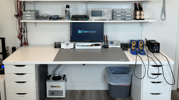
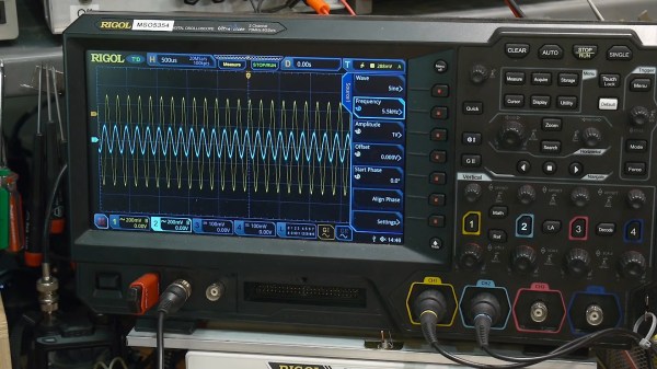
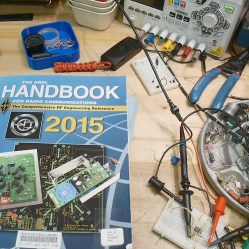
Setting up an electronics work area is a highly personal and situational affair, with many interesting problems to be solved, and for many of us, significant budget constraints. The requirements for electronics development vary wildly depending upon the sort of work to be undertaken, but there is core equipment that many of us would consider a bare minimum for usability. [Badar Jahangir Kayani] is at the start of his career as an electrical engineer, and has documented the kitting out of his personal work areas for others to learn from.

As we already touched upon, the cost is often the main driving factor determining what we end up with, and this cost-vs-performance/quality tradeoff is what makes some of us fret over a buying decision. Buying secondhand off eBay is an option, but a lack of warranty and the unknowable condition are not great selling points.
[Badar] has a good grasp of the basic concepts of usability, such as keeping the most frequently used tools, instruments, and components out in the open. Less frequently used stuff is stored in drawers, bins, and compartment boxes. Buying the same storage systems keeps things as consistent as much as possible since it makes storing them easier. We were particularly interested in the use of the cloud-based database solution, Airtable used to create a parts database for minimal outlay.
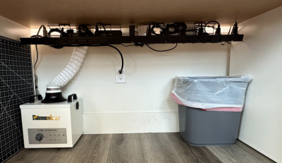
There is also a lot of detail about how to walk that cost/quality/performance tightrope and get the best-valued gear currently on the market. Some notable examples are the UNI-T UT61E Digital Multimeter for general test use, the Controleo3 reflow controller for SMT assembly, and the Omnifixo OF-M4 magnetic fixament kit for that fiddly wiring part. [Badar] also recommends the FumeClear Solder Fume Extractor, although they lament that particular bit of kit is still under evaluation.
Obviously, we’ve talked about work areas a lot on these pages, like this time. For those with more space, this flippin’ awesome bench will be of interest, and if space is tight (or travel is a regular thing) might we suggest this 3D printed DIN-rail mounting cube as a starting point?

