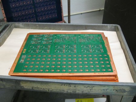
Although not a hack in itself, many of you may be interested in seeing how a printed circuit board is made in the manufacturing world. This tour of Advanced Circuits does a good job of explaining the process. The article explains how a PCB will go through a CAD/CAM review, drilling, deburring, and the various chemical etch, plating, and curing processes.
Although many hackers make their own PCBs, having it professionally done can be a good option depending on how many copies are needed. One benefit of this is that PCBs can be checked by an optical inspection process, or even by a “flying lead” machine which works by contacting leads automatically in a computer controlled setup.
A video of this incredible machine is included after the break. Around 0:26 is when it really starts to get going. Continue reading “Tour Of Advanced Circuits – A PCB Manufacturer”

