A Complete Desktop PCB Etching Station

Right now you can get a custom circuit board delivered to your door in about a week for just a few dollars. There’s little reason to make your own circuit boards at home anymore, but when you need a board now, you want to have that capability. [Tuval Ben Dosa] designed a complete PCB etching station that is the perfect tool for making printed circuit boards at home. It’s got everything you need for the perfect etch, and with this setup you can make a board in hours instead of waiting for days.

The chemistry for any etching setup is important, and in recent years the entire community has moved from ferric chloride to copper chloride for a very good reason: you can recharge copper chloride etchant by bubbling oxygen (or air) through it, whereas ferric chloride is a one-use etchant.

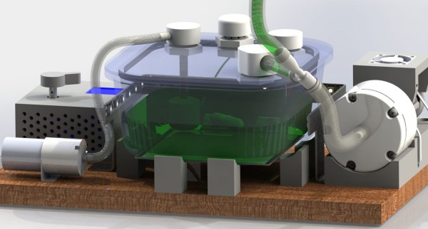
The mechanical part of this build consists of an airtight glass food container sitting on top of a PCB heating element not unlike the heated bed of a 3D printer. Along with that is an I2C temperature sensor encased in a silicone tube, a stir bar, diaphram pump, and a few pumps to blow air into the etchant and pump out the chlorine gas generated. This is controlled by a small microcontroller with a UI consisting of just an encoder and OLED display.

If you’re looking for builds that will etch copper and brass at home, this has been something that has been done before. The Etchinator is a fantastic build capable of making everything from printmaking plates to printed circuit boards. That’s a build that requires a lot of work, and this small, compact etching station does everything you need without taking up too much space in the shop. Check out the video below.

Continue reading “A Complete Desktop PCB Etching Station”

What’s The Deal With Square Traces On PCBs

When designing a printed circuit board, there are certain rules. You should place decoupling capacitors near the power pins to each chip. Your ground planes should be one gigantic fill of copper; two ground planes connected by a single trace is better known as an antenna. Analog sections should be kept separate from digital sections, and if you’re dealing with high voltage, that section needs to be isolated.

One that I hear a lot is that you must never put a 90-degree angle on a trace. Some fear the mere sight of a 90-degree angle on a PCB tells everyone you don’t know what you’re doing. But is there is really no greater sin than a 90-degree trace on a circuit board?

This conventional wisdom of eschewing 90-degree traces is baked into everything we know about circuit board design. It is the first thing you’re taught, and it’s the first thing you’ll criticize when you find a board with 90-degree traces. Do square traces actually matter? The short answer is no, but there’s still a reason we don’t do it.

Continue reading “What’s The Deal With Square Traces On PCBs”

EasyEDA Hack Chat With Dillon He

Join us Wednesday at 5:00 PM Pacific time for the Easy EDA Hack Chat with Dillon He!

Note the different time than our usual Hack Chat slot! Dillon will be joining us from China.

Since the birth of electronic design automation in the 1980s, the universe of products to choose from has grown tremendously. Features from schematic editing to circuit simulation to PCB design and autorouting can be found in every permutation imaginable, and you’re sure to find something that fits your needs, suits your budget, and works on your platform.

Dillon He started EasyEDA back in 2010 with Eric Cui, and since then the cloud-based EDA tool has become a popular choice. From working across teams to its “run anywhere” capabilities, EasyEDA has become the go-to tool for hundred of thousands of designers. Dillon will drop by the Hack Chat to answer all your questions about EasyEDA — how it started, where it is now, and what we can expect in the future.

join-hack-chatOur Hack Chats are live community events in the Hackaday.io Hack Chat group messaging. This week we’ll be sitting down on Wednesday, June 19 at 5:00 PM Pacific time. If time zones have got you down, we have a handy time zone converter.

Click that speech bubble to the right, and you’ll be taken directly to the Hack Chat group on Hackaday.io. You don’t have to wait until Wednesday; join whenever you want and you can see what the community is talking about.


Visualizing How Signals Travel In A PCB

If you play with high speed design for long enough, eventually you’re going to run into clock skew and other weird effects. [Robert Feranec] recently ran into this problem and found an interesting solution to visualizing electric fields in a PCB.

A word of warning before we dig into this, for most of the projects we see on Hackaday something like this is completely superfluous. There aren’t many people dealing with high speed interfaces here, and there aren’t many people dealing with 100 Gigabit per second data links, period. That said, it’s not unheard of, and at the very least it’s interesting to look at.

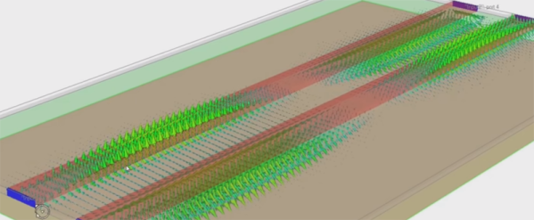
The basics of this video is simulating the signals visually in a differential pair on a (virtual) printed circuit board. The software for this is Simbeor, and [Robert] talked to the founder of the company behind this software after watching a video on simulating electric fields in differential traces. This software does what it says, and is a great illustration of why differential pairs must have the same length.

While this might not be for everyone, it is a fantastic visualization of signals in high-speed design that goes above and beyond what you would expect from a Spice simulation. Even if you’re not doing high-speed design, you may someday and it’s never too soon to get an intuitive understanding of how electrons work.

Continue reading “Visualizing How Signals Travel In A PCB”

Flexible PCBs Hack Chat With OSH Park

Join us Thursday at noon Pacific time for the Flexible PCBs Hack Chat with Drew and Chris from OSH Park!
Note the different day from our usual Hack Chat schedule!
Printed circuit boards have been around for decades, and mass production of them has been an incalculable boon to the electronics industry. But turning the economics of PCB production around and making it accessible to small-scale producers and even home experimenters is a relatively recent development, and one which may have an even broader and deeper impact on the industry in the long run.

And now, as if professional PCBs at ridiculous prices weren’t enough, the home-gamer now has access to flexible PCBs. From wearables to sensor applications, flex PCBs have wide-ranging applications and stand to open up new frontiers to the hardware hacker. We’ve even partnered with OSH Park in the Flexible PCB Contest, specifically to stretch your flexible wings and get you thinking beyond flat, rigid PCBs.

join-hack-chatOur Hack Chats are live community events in the Hackaday.io Hack Chat group messaging. This week we’ll be sitting down on Thursday, May 23 at 12:00 PM Pacific time. If time zones have got you down, we have a handy time zone converter.

Click that speech bubble to the right, and you’ll be taken directly to the Hack Chat group on Hackaday.io. You don’t have to wait until Thursday; join whenever you want and you can see what the community is talking about.

Analog Failures On RF Product Cause Production Surprise

A factory is a machine. It takes a fixed set of inputs – circuit boards, plastic enclosures, optimism – and produces a fixed set of outputs in the form of assembled products. Sometimes it is comprised of real machines (see any recent video of a Tesla assembly line) but more often it’s a mixture of mechanical machines and meaty humans working together. Regardless of the exact balance the factory machine is conceived of by a production engineer and goes through the same design, iteration, polish cycle that the rest of the product does (in this sense product development is somewhat fractal). Last year [Michael Ossmann] had a surprise production problem which is both a chilling tale of a nasty hardware bug and a great reminder of how fragile manufacturing can be. It’s a natural fit for this year’s theme of going to production.

Surprise VCC glitching causing CPU reset

The saga begins with [Michael] receiving an urgent message from the factory that an existing product which had been in production for years was failing at such a high rate that they had stopped the production line. There are few worse notes to get from a factory! The issue was apparently “failure to program” and Great Scott Gadgets immediately requested samples from their manufacturer to debug. What follows is a carefully described and very educational debug session from hell, involving reverse engineering ROMs, probing errant voltage rails, and large sample sizes. [Michael] doesn’t give us a sense for how long it took to isolate but given how minute the root cause was we’d bet that it was a long, long time.

The post stands alone as an exemplar for debugging nasty hardware glitches, but we’d like to call attention to the second root cause buried near the end of the post. What stopped the manufacturer wasn’t the hardware problem so much as a process issue which had been exposed. It turned out the bug had always been reproducible in about 3% of units but the factory had never mentioned it. Why? We’d suspect that [Michael]’s guess is correct. The operators who happened to perform the failing step had discovered a workaround years ago and transparently smoothed the failure over. Then there was a staff change and the new operator started flagging the failure instead of fixing it. Arguably this is what should have been happening the entire time, but in this one tiny corner of the process the manufacturing process had been slightly deviated from. For a little more color check out episode #440.2 of the Amp Hour to hear [Chris Gammell] talk about it with [Michael]. It’s a good reminder that a product is only as reliable as the process that builds it, and that process isn’t always as reliable as it seems.

Prototyping PCBs With Electrical Discharge Machining

Here at Hackaday, we thought we’d seen every method of making PCBs: CNC machining, masking and etching with a variety of chemicals, laser engraving, or even the crude but effective method of scratching away the copper with a utility knife. Whatever works is fine with us, really, but there still does seem to be room for improvement in the DIY PCB field. To whit, we present rapid PCB prototyping with electrical discharge machining.

Using an electric arc to selectively ablate the copper cladding on a PCB seems like a great idea. At least that’s how it seemed to [Jake Wachlin] when he realized that the old trick of cutting a sheet of aluminum foil using a nine-volt battery and a pencil lead is really just a form of EDM, and that the layer of copper on a PCB is not a million miles different from foil. A few experiments with a bench power supply and a mechanical pencil lead showed that it’s relatively easy to blast the copper from a blank board, so [Jake] took the next logical step and rigged up an old 3D-printer to move the tool. The video below shows the setup and some early tests; it’s not perfect by a long shot, but it has a lot of promise. If he can control the arc better, this homebrew EDM looks like it could very rapidly produce prototype boards.

[Jake] posted this project in its current state in the hopes of stimulating a discussion and further experimentation. That’s commendable, and we’d really love to see this one move along rapidly. You might start your brainstorming by looking at this somewhat sketchy mains-powered EDM, or look into the whole field in a little more detail.

Continue reading “Prototyping PCBs With Electrical Discharge Machining”